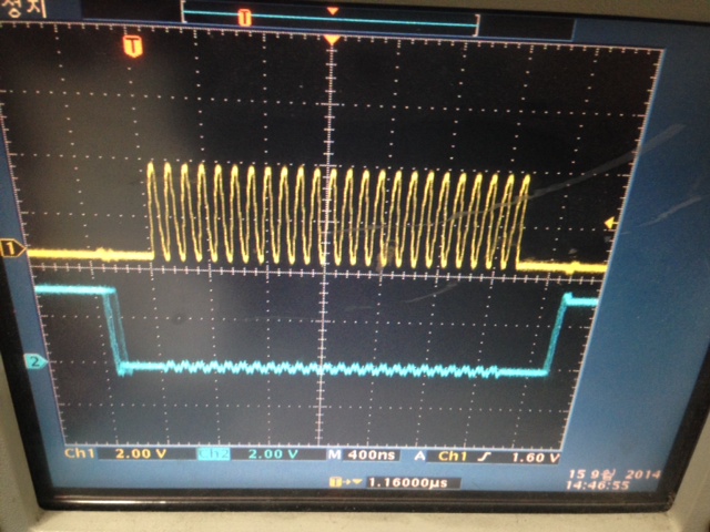
This thread has been locked.

If you have a related question, please click the "Ask a related question" button in the top right corner. The newly created question will be automatically linked to this question.

not operate DAC8760

Other Parts Discussed in Thread: DAC8760

DATA IN                                                                                               SCLK

SCLK                                                                                                   LATCH

I am using SPICLK(rising edge with delay)

I

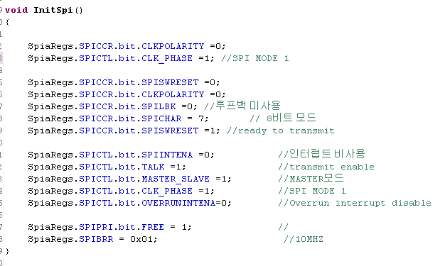
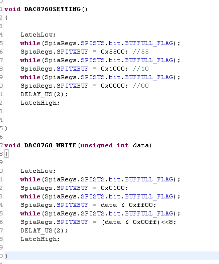
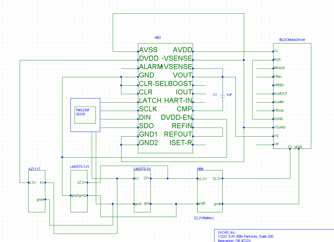
I am working for using DAC8760 with TMS230F28335

but DAC8760 not operated

I don`t know why DAC8760 not operated.

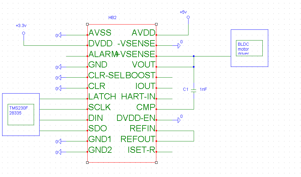
DAC8760 pin connect(TSSOP-24) : only using Vout

1. AVSS : gnd

2. DVDD : 3.3V

7~10 : connected 28835

11,12 : gnd

14,15 : connect each other

16:gnd

17,21 : 17-----------1nF-------------21 connect

21,22 : connect

23 :connect

24:5V

if I did a incorrect work, i hope you know correct method using DAC8760

below DSP code

  • Kang,

    You clock phase and polarity settings are correct. The protocol you are implementing to communicate with the device also looks correct, both in code and in the oscilloscope captures you have provided. There is considerable ringing and cross-talk in your SPI signals but I do not think that is the cause of this issue.

    It would be helpful if you could provide a schematic to double check your hardware rather than words describing the connections in the design.

    In the oscilloscope capture you provided you are writing address byte 0x01 with data 0xFFFF, which corresponds to writing full-scale data to the DAC Data register. Is this the complete write sequence that you are using to test communication with the device?

  •  

    schematic include

     you say I am writing adreess  byte 0x01 with data 0xFFFF

    becasue TMS230F28335 has SPI with sending 16bit

    but DAC8760 has 24bit adresss

    so I am sending each 8bit

    and I checked sending correct data by osciloscope

    and is it right including schematic??

  • Kang,

    Thanks for following up. More comments for you:

    kang jeonmook said:

     you say I am writing adreess  byte 0x01 with data 0xFFFF

    becasue TMS230F28335 has SPI with sending 16bit

    but DAC8760 has 24bit adresss

    so I am sending each 8bi

    Understood - we discussed the format you are using to communicate with the device in a previous E2E thread. The method you are using to communicate with the device looks good in both code and in the oscilloscope captures that you provided.

    The oscilloscope capture you provided writes the 24-bit word 0x01FFFF which writes full-scale to the DAC Data Register. If this is the only write that you perform I would not expect for the device to respond in any way because neither the voltage or current outputs are enabled. In order to enable the analog outputs you need to write a '1' to bit 12 in the Control Register (address 0x55). With the outputs active you should see the voltage or current output respond to data placed in the DAC Data Register. The output mode that is active is set by the RANGE bits in the Control Register.

    kang jeonmook said:
    and is it right including schematic??

    Functionally the schematic looks okay. There are several off-page connectors that make some details difficult to access. I would suggest that decoupling capacitors are included on AVDD and DVDD. A small decoupling cap should also be included on the REFIN to REFOUT connection.

  • I am solved.

    problem didnt connect analoge and digital with seperated

    but problem appear.too


    as you see, even though I am setting 0~5V range in control register

    but this picture show Vout is 300mV~7V

    so I did set gain register and zero register..

    but DAC8760 is still showing 300mV~7V

  • Kang,

    Is the oscilloscope ground connected to the board ground?

    Can you measure the reference voltage?

  • i am using a internal reference

  • Kang,

    You can measure the internal reference at the REFOUT pin.

  • Kang,

    You have verified that your system and measurement equipment are grounded correctly?

  • when I sended 0xffff to data register, REFout is 5V

    when I sended 0x0000 to data register, REFout is 0V 

  • Kang,

    Writing to the DAC Data Register should not have any impact on the output of the reference voltage. Do you have an evaluation module for the DAC8760? If so I would suggest that you verify your SPI communication using the known-working EVM. Then we can move on to debugging the analog issues on your PCB that are leading to accuracy issues on the outputs.

  • I am mistaken to measure REFout

    REFout is always 5V

     and when I am sending 0x0000 to 0xffff, I am looked to jumping 3.3V to 7V immediately

    cf) AVDD is 7V, not 5V

  • Kang,

    Can you provide a full-schematic of the board you are using to make these measurements? If you could share the layout as well that would be helpful. I'd like to also know exactly where you are making the measurement as well (Where is the oscilloscope lead placed? Where is the ground lead of the oscilloscope placed?).

  •  

    when I measered  Vout,  I placed on VSGND of motordriver

    below address appeares motordriver spec

    http://www.motorplus.kr/shop/goods/goods_view.php?&goodsno=597&category=003002

  • Kang,

    Have you made any measurements with the DAC unloaded?

  • Yes, but the result is identical

    and sounds weird, if AVDD is 12V and I send 0x01ffff, Vout is 12V

                                       if AVDD is 5V and I send 0x01ffff, Vout is 5V

    I don`t know what problem is

    cf)REFOUT is 5V

  • Kang,

    Do you have any way of sharing the layout of this design?

    What is the output voltage at zero-scale for each of those cases? What about mid-scale?

    The only way the output voltage should be tracking with the supply voltage is if the output amplifiers are operating open loop and simply hitting their rails. If this is the case we should see the full-scale output regardless of what the input code is.

  • I don`t know what means zero-scale??

    zero scale is 0V, isn`t it??

  • Kang,

    Zero-scale means the DAC data register contains 0x0000. Mid-scale is 0x8000. Full-scale is 0xFFFF. Please let me know what the output voltage is for each DAC data word.

    As I have mentioned, providing the layout would be helpful as well.

  • layout means circuit diagram?

  • Kang,

    Layout means the GERBER files or project files used to create the printed circuit board (PCB). 

  • if I send 0x8888, Vout is 2.5V

    if I send 0x0000, Vout is 0V

    but if I send 0xffff, Vout is 7V

    1537.Schematic1.sch

  • measurement video

    increase sending value until 0xffff

  • i`m waiting you

  • Kang,

    kang jeonmook said:

    if I send 0x8888, Vout is 2.5V

    if I send 0x0000, Vout is 0V

    but if I send 0xffff, Vout is 7V

    What is AVDD in this case? 7V? Previously you mentioned if AVDD is 5V then full-scale data output is 5V. Similarly if AVDD was 12V full-scale data output is 12V.

    What is the thermal pad connected to?

    The PCB layout would still be helpful. The schematic you shared is not the layout.

  • AVDD is 7V

    thermal pad was connected to  AVSS(GND)

  • PCB layout is nothing 

    because I am soldering the circuit board directly

    help me...ㅠㅠ

  • Kang,

    I see several independent ground connections in your schematic, are all of these grounds connected to one another eventually? All of the grounds need to be connected to one another or you have several floating potentials in this design that is going to cause either parametric degradation, complete lack of functionality, or conceivably permanent damage to the components.

    If you do not have a layout then the schematic you have shared is relatively meaningless. There could be any number of issues in the connections that you have made manually that is leading to a considerable gain error on the voltage output.