This thread has been locked.

If you have a related question, please click the "Ask a related question" button in the top right corner. The newly created question will be automatically linked to this question.

setup ADS1240E using pic18f46k22

Other Parts Discussed in Thread: ADS1240

hi all,

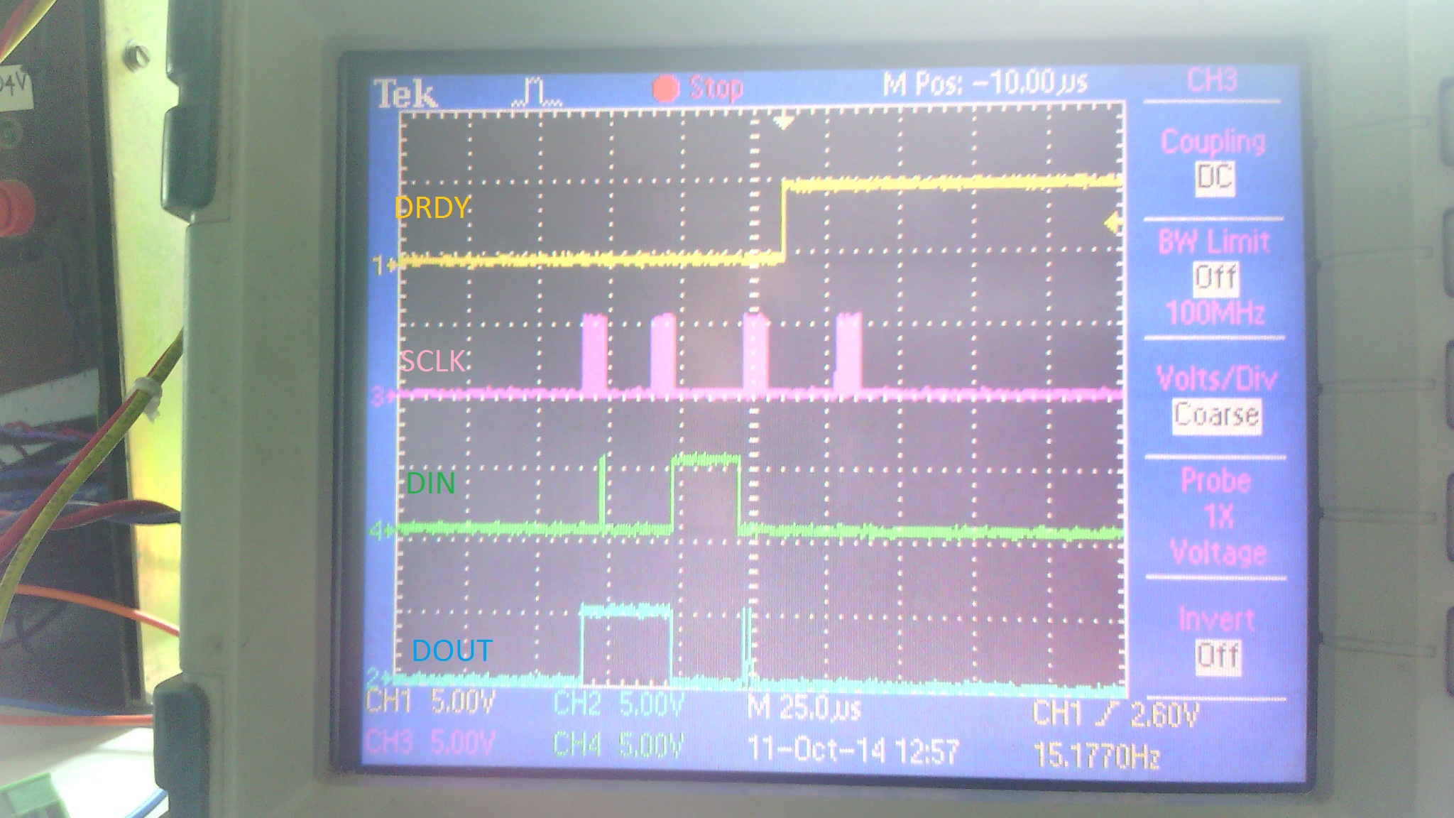
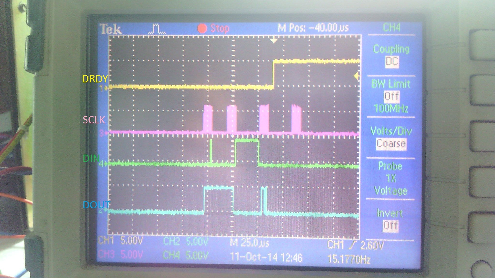
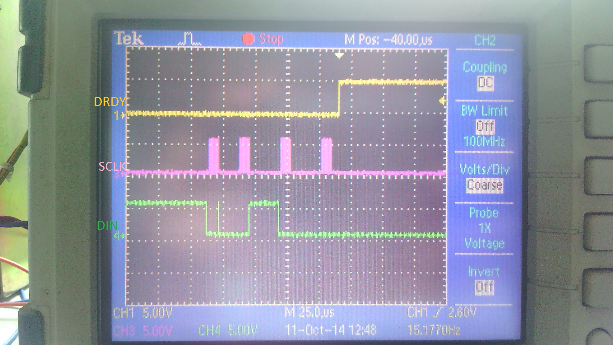
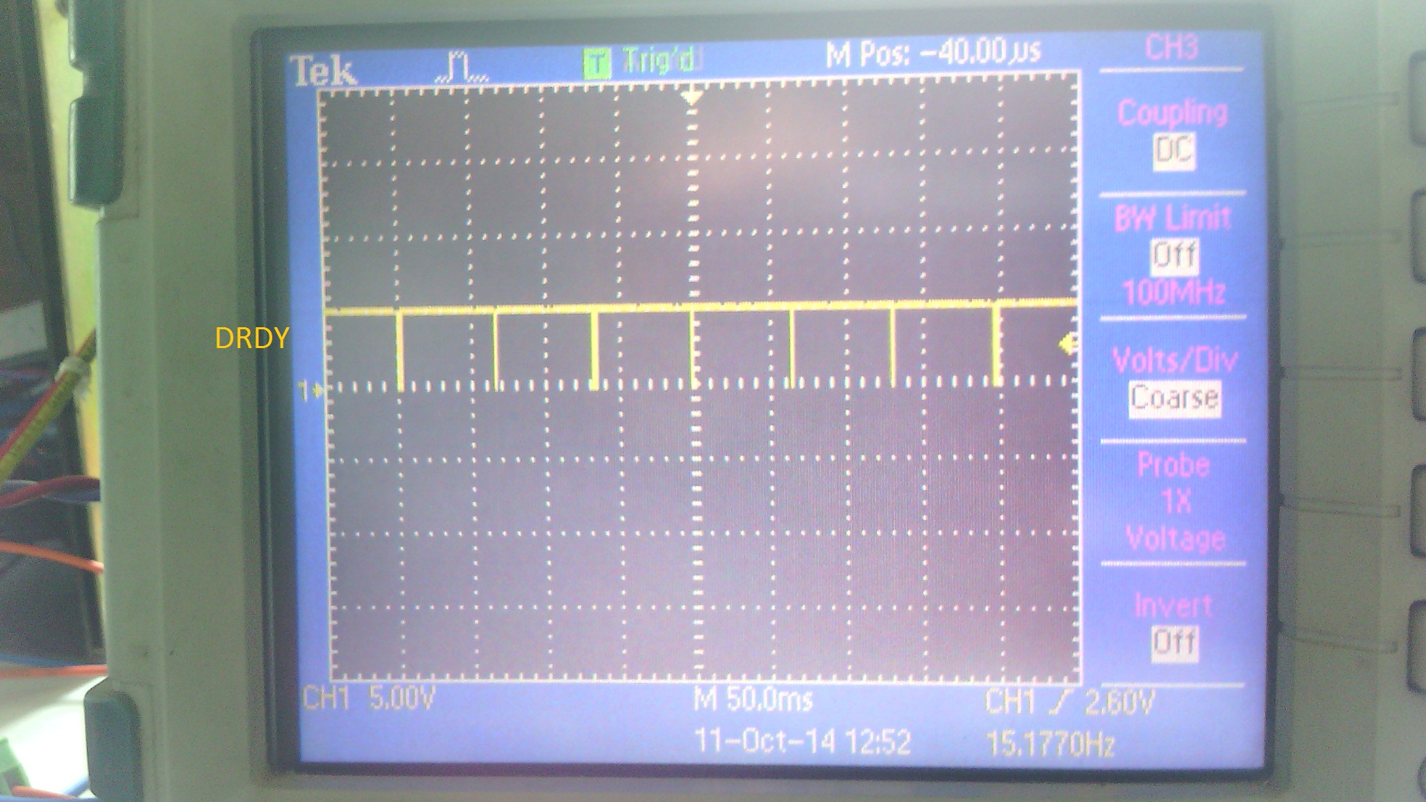
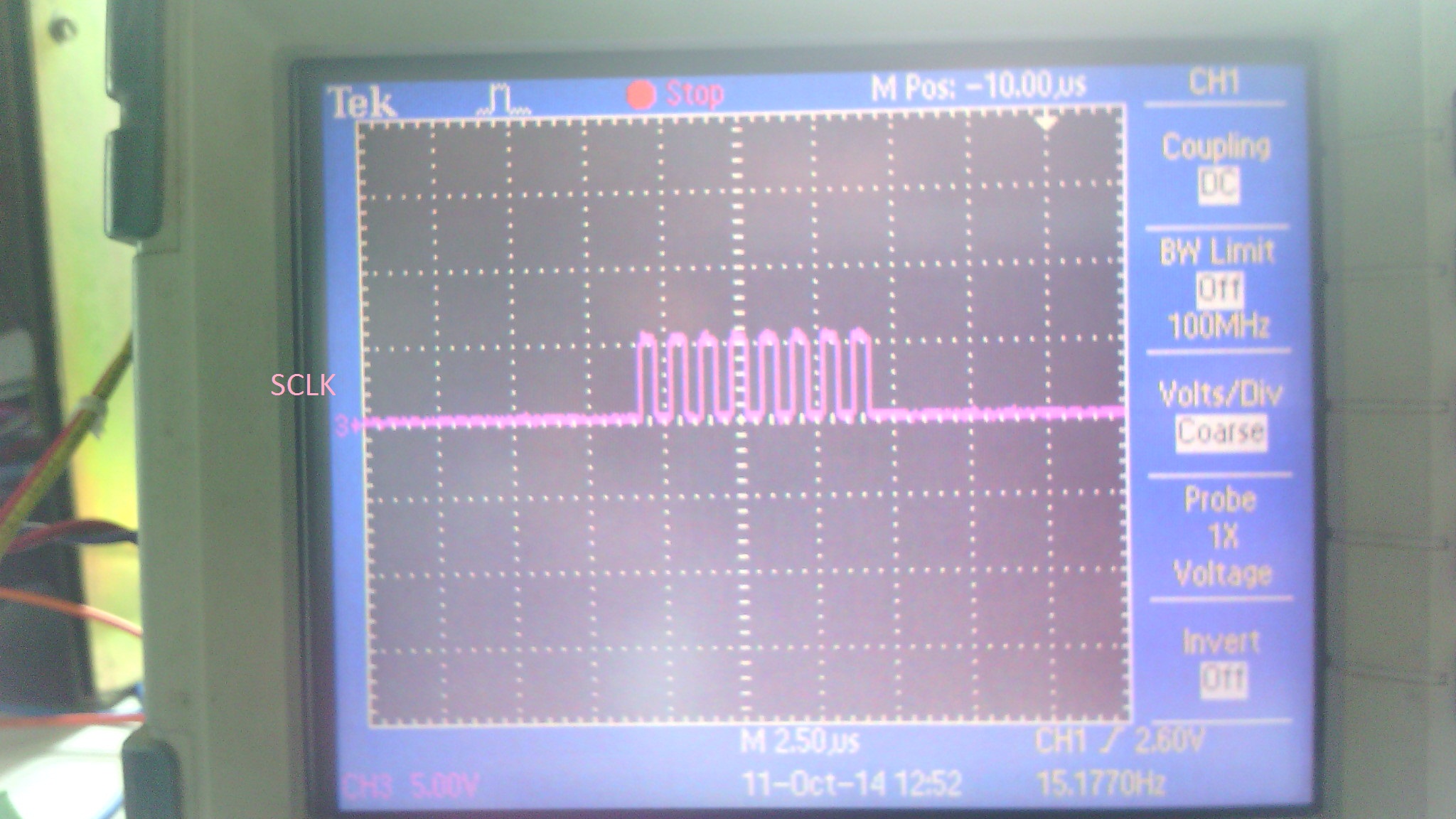
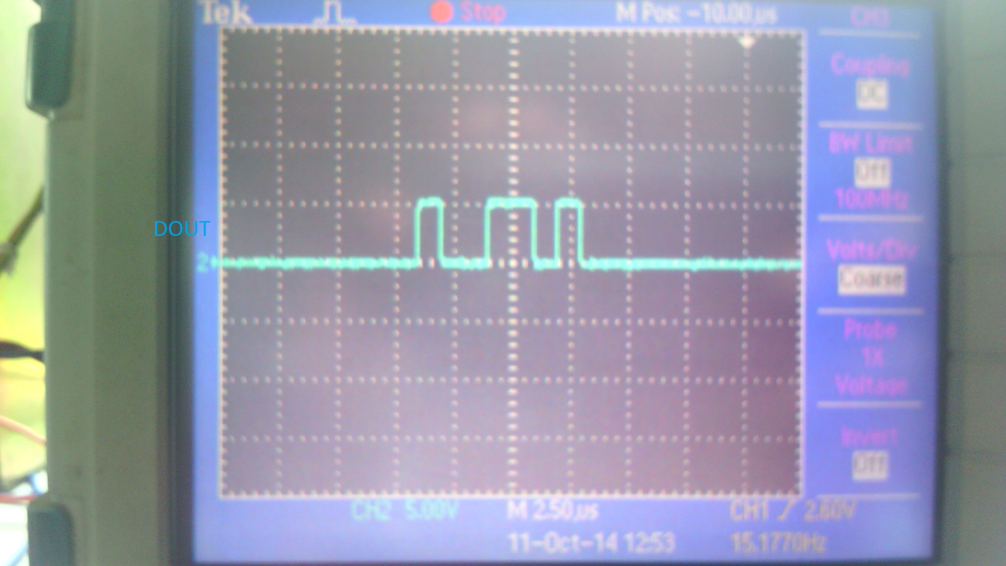
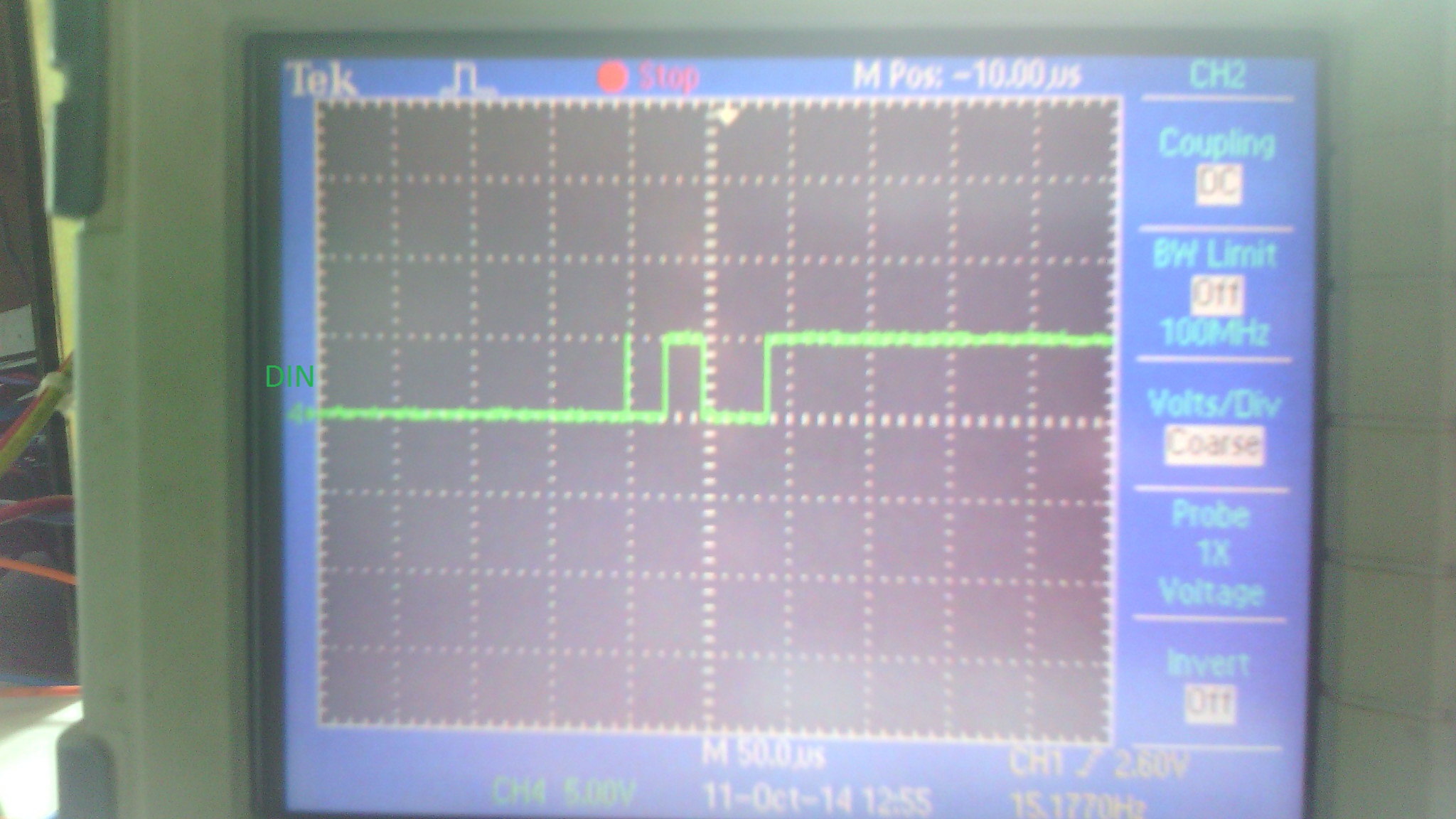
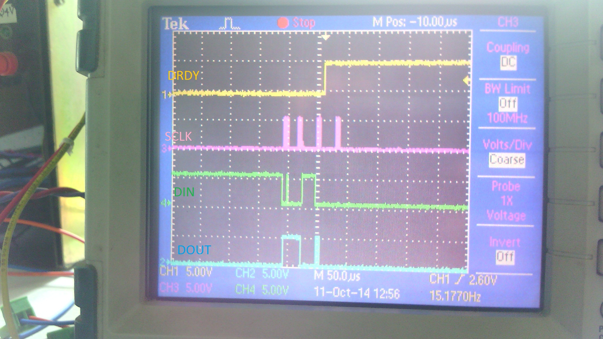
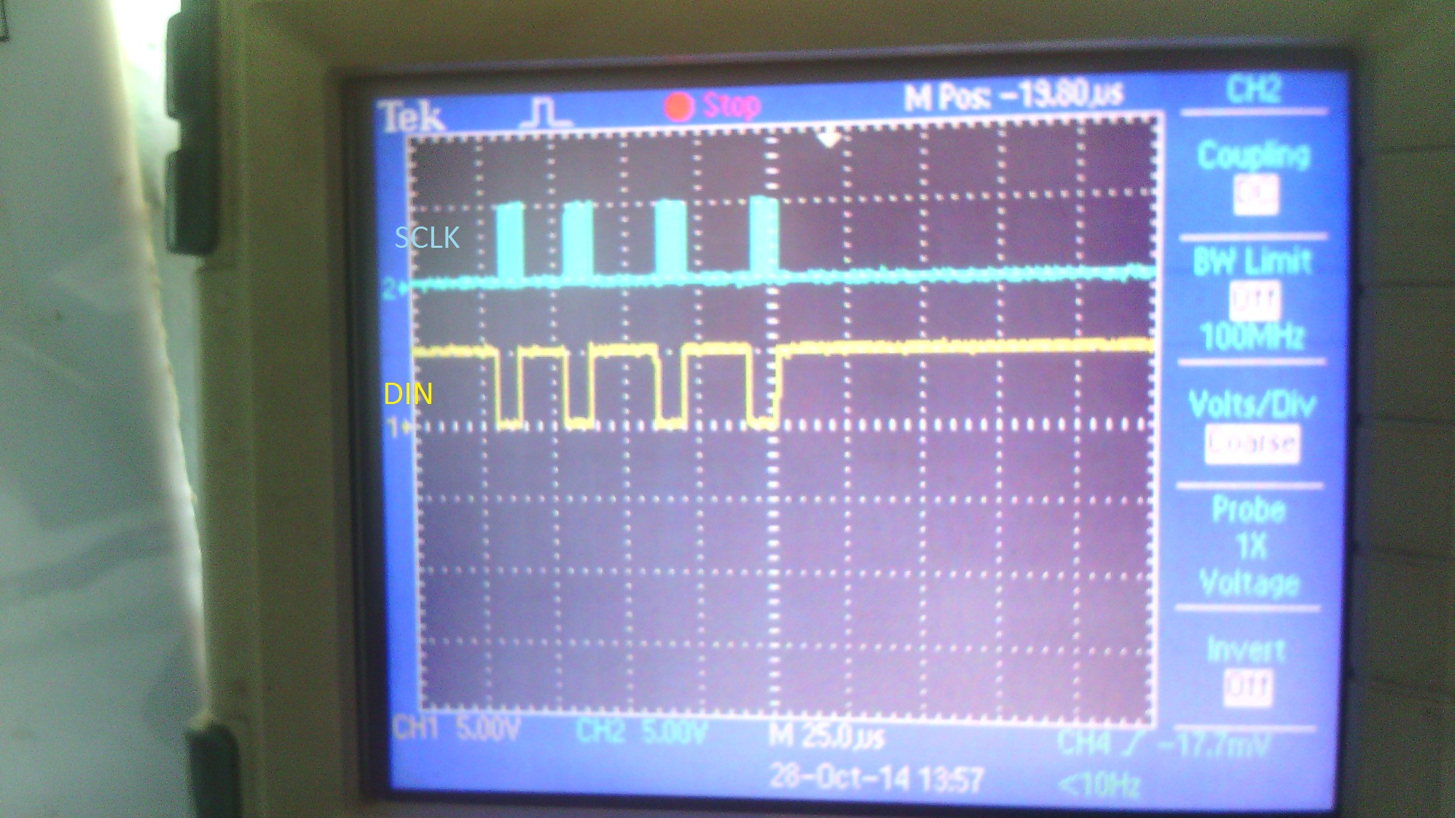
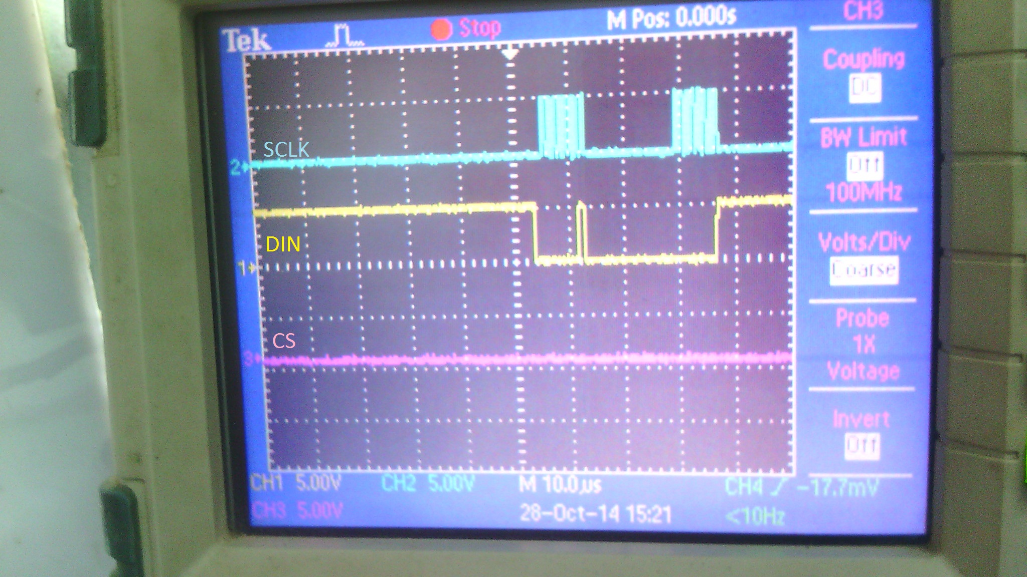
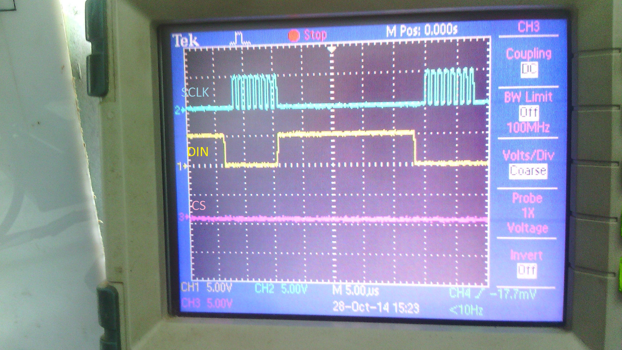
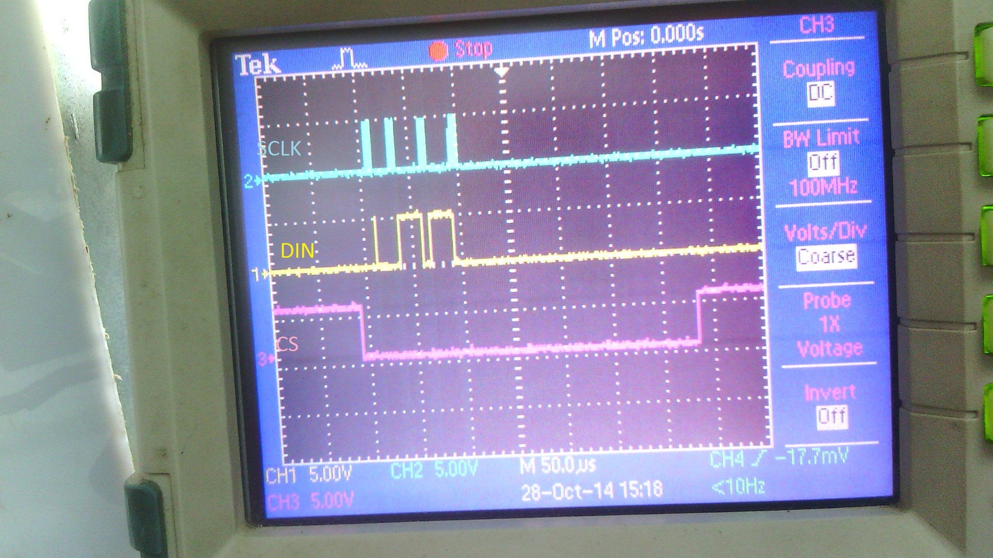
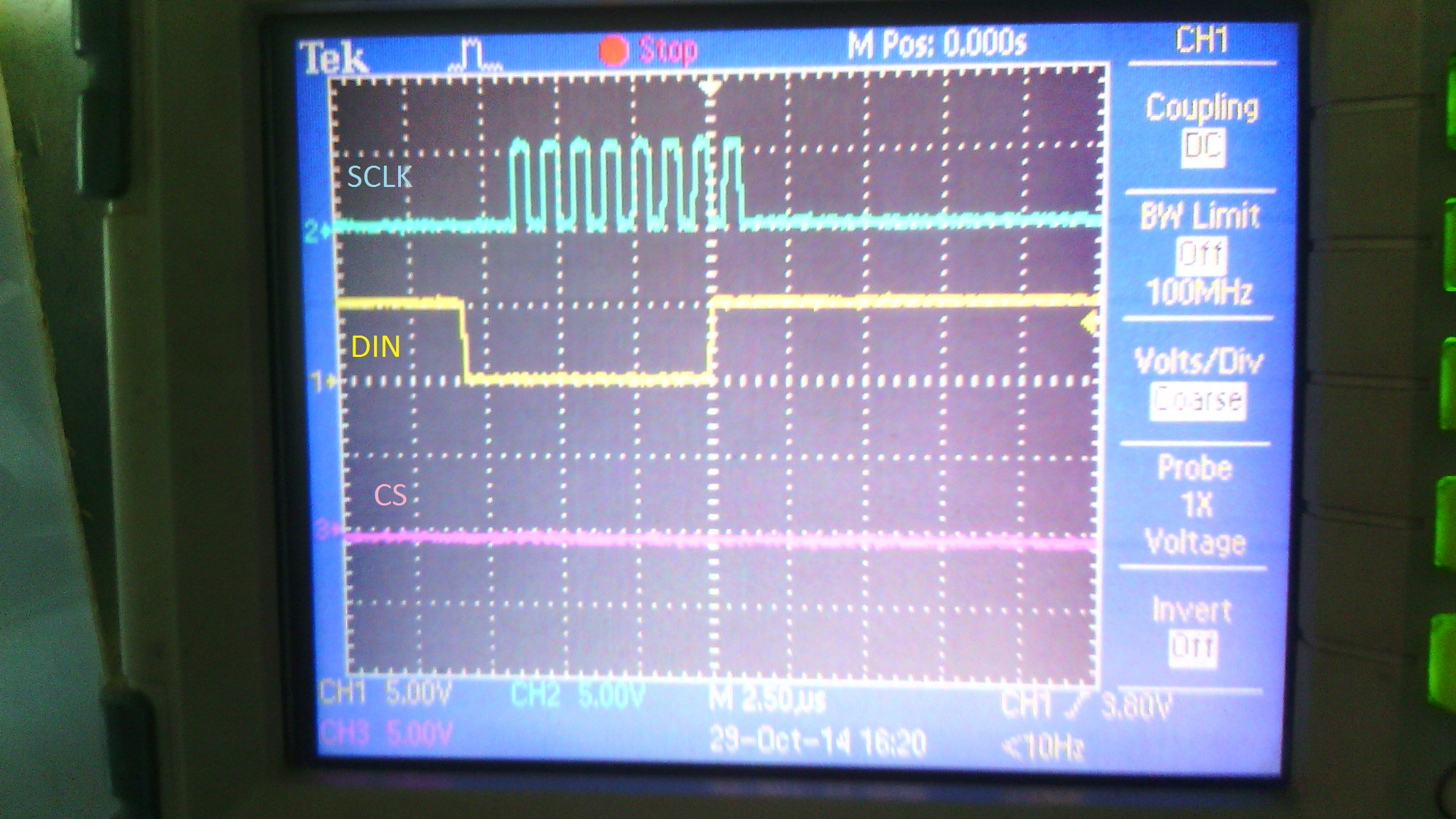
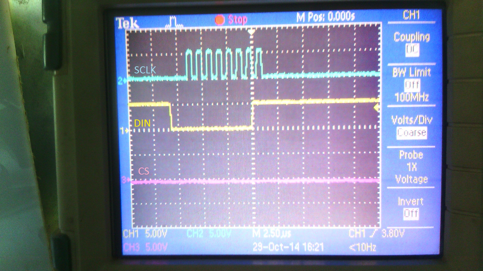
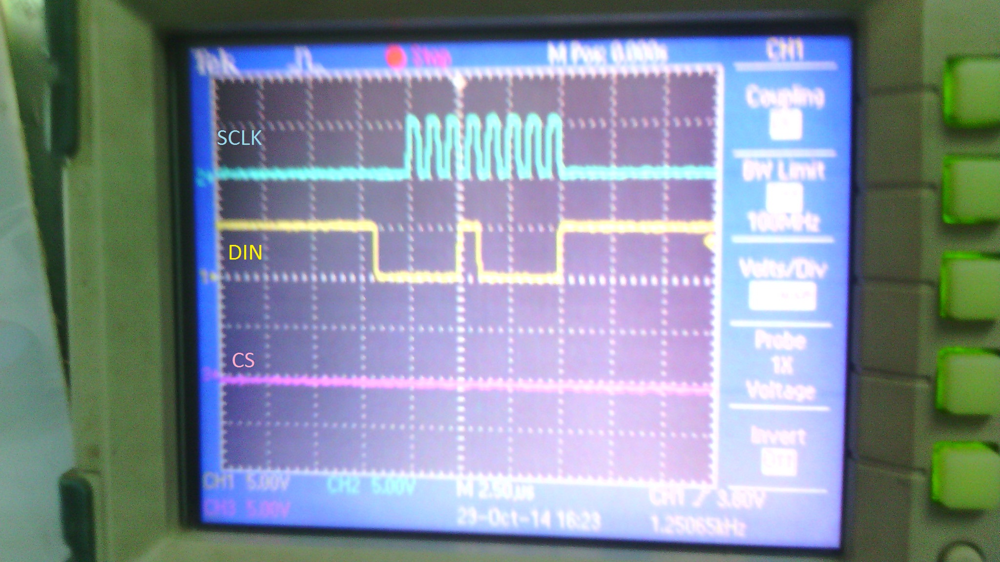
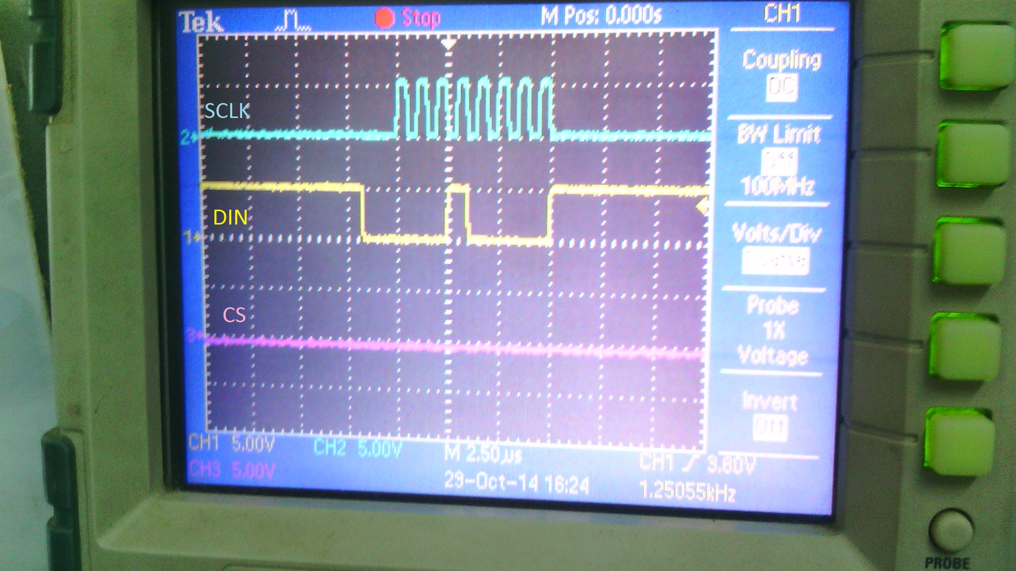
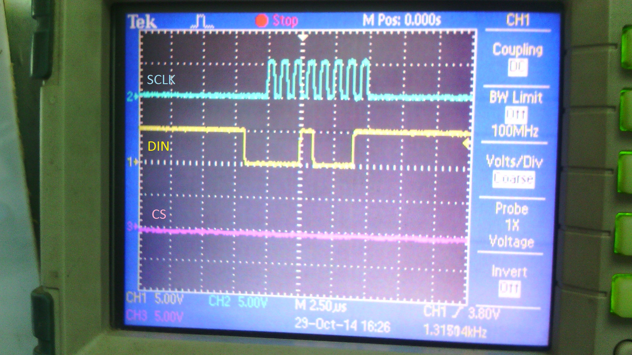
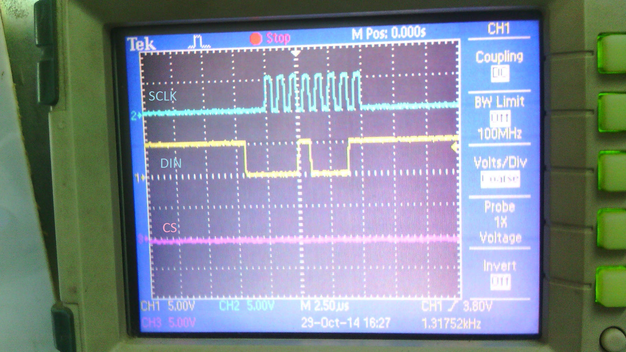
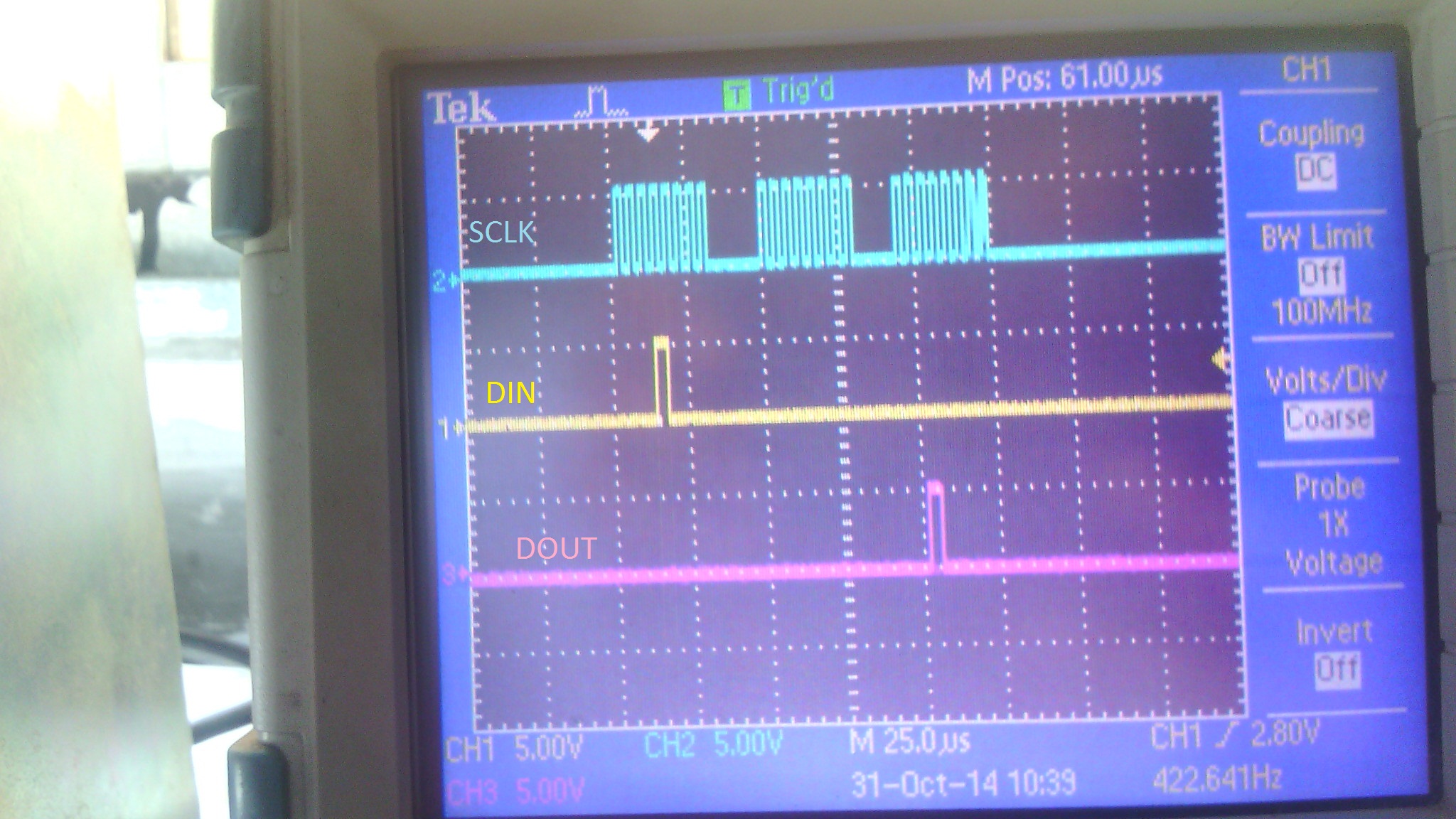
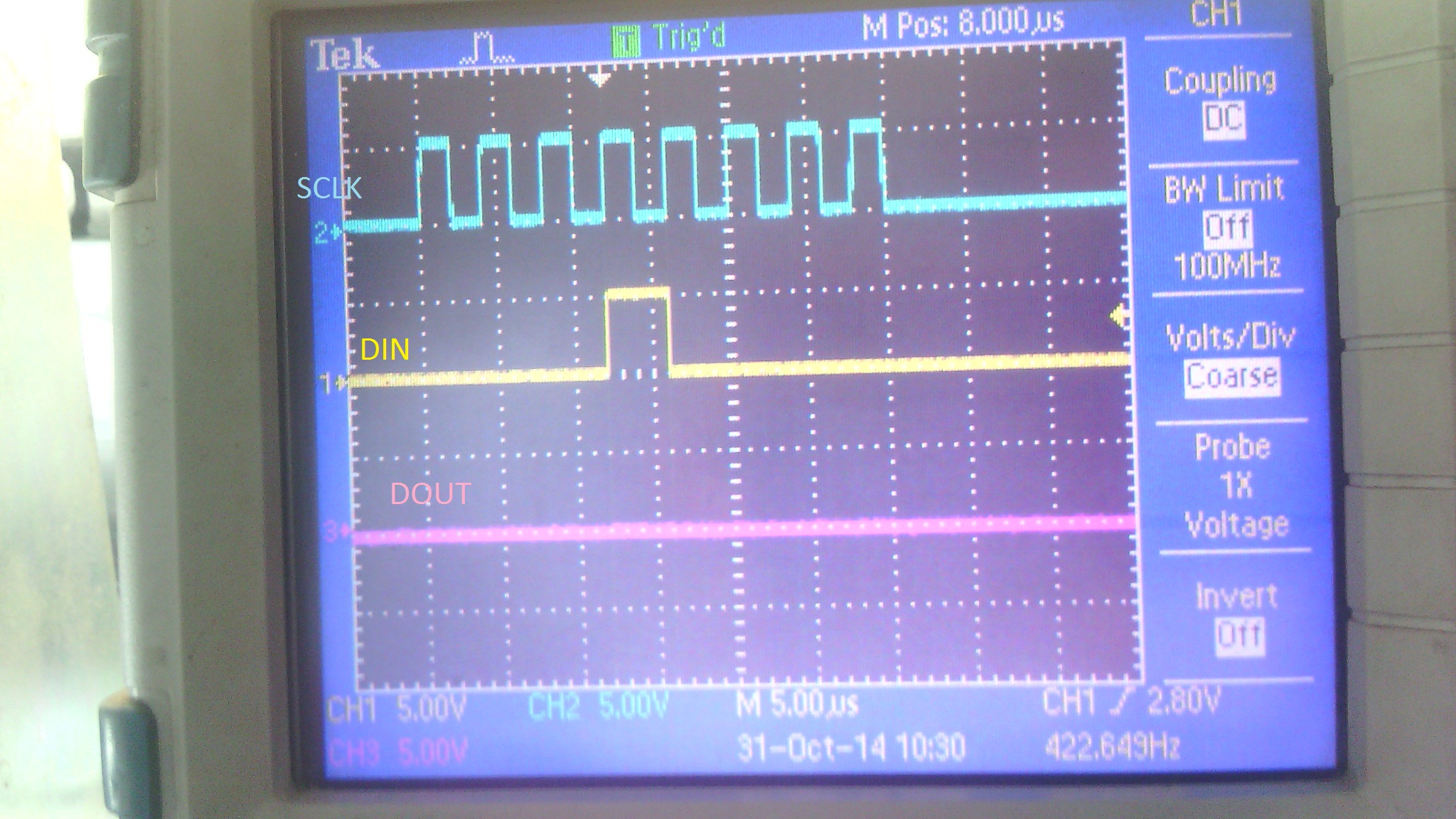
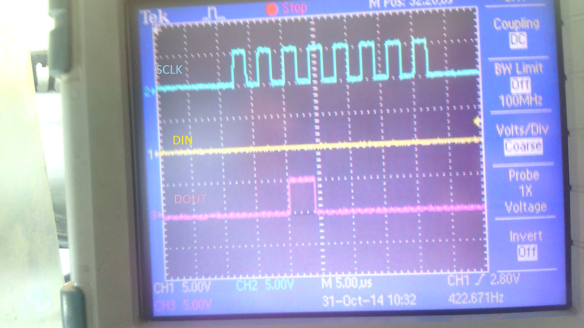
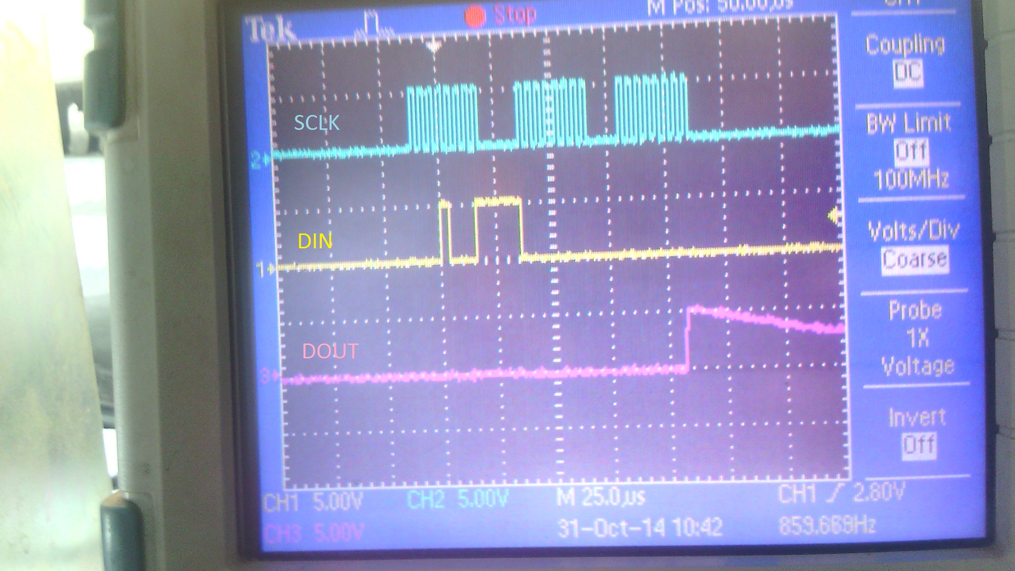
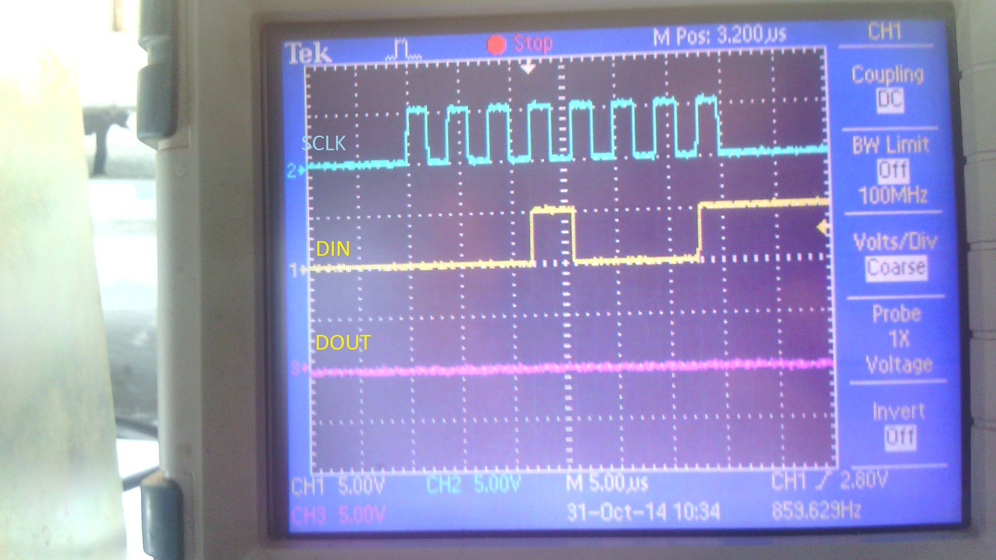
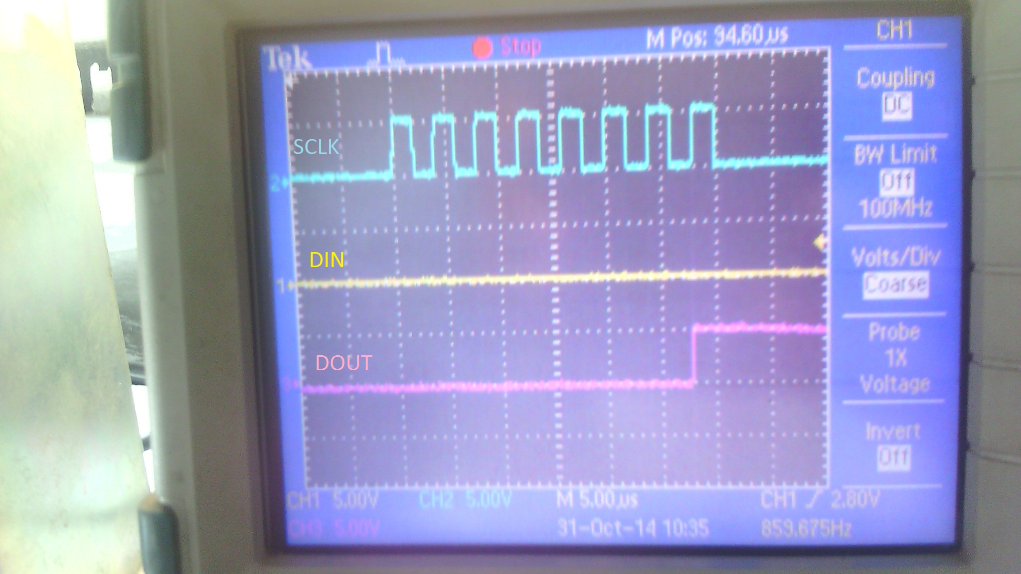
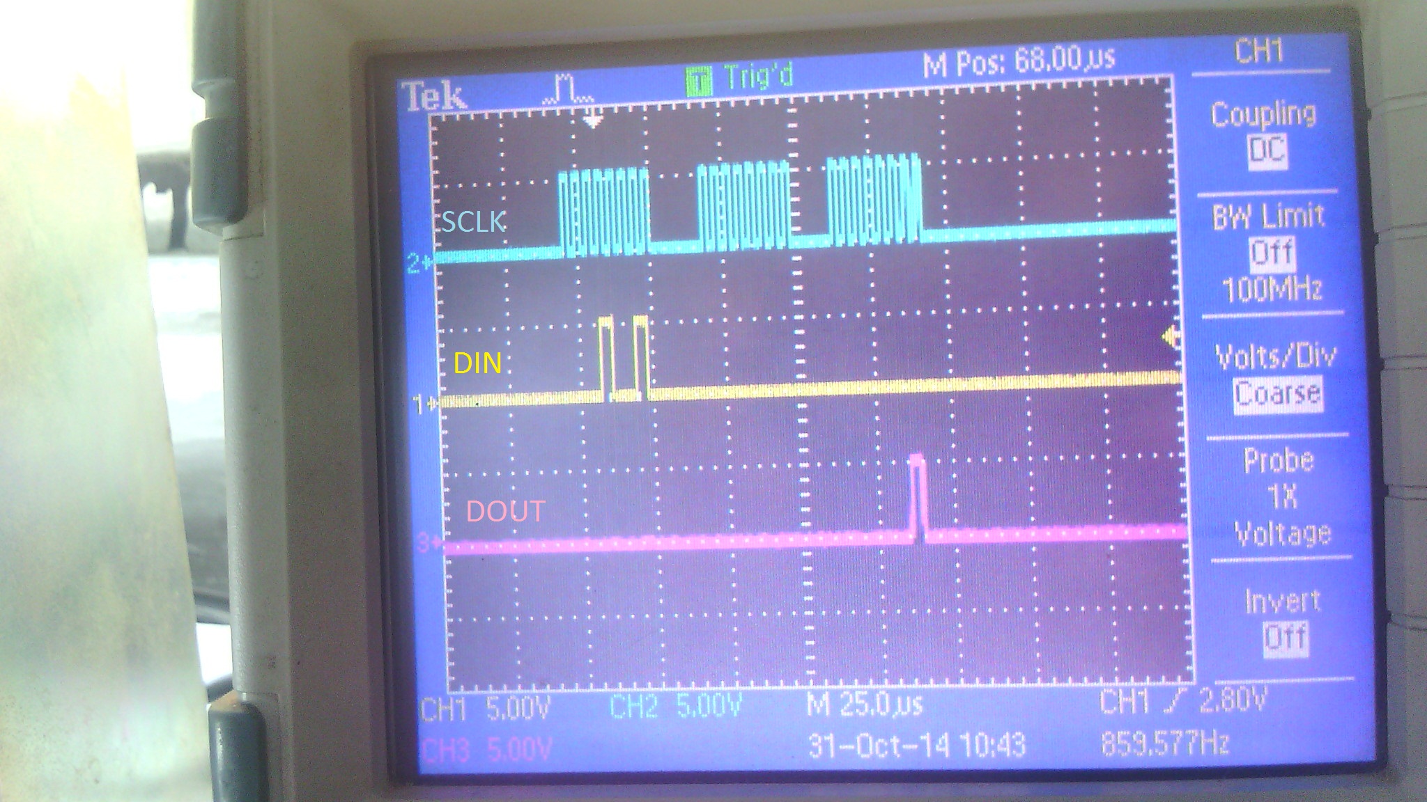
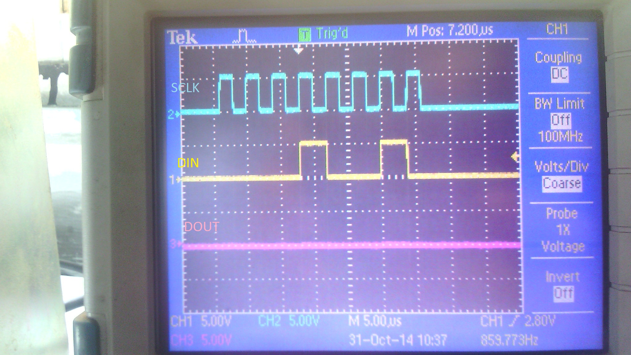
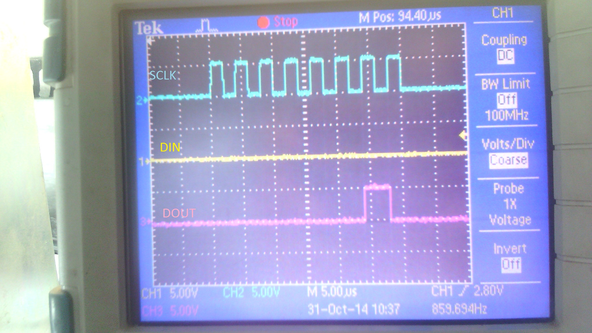
 i am mahesh working on ADS1240E for bridge sensor o/p processing . i was done set up for ADS1240E as per application note from texas i.e. slaa125a. and check waveforms on DSO.but i am not getting desire waveform for DRDY pin. i.e. i have set data rate as 3.75 Hz but on DSO i am getting it as 15 Hz only. and also there is no change in gain if i have changed gain from 1 to 2 or 4.

so help me to set up initialization of ADS1240E.

  • Hi Mahesh,

    Since you're able to look at the waveforms with a DSO for the communication to the ADS1240, could you please post a screen shot of this?


    I would write commands one register at a time and post the signals for /CS, SCLK, DIN and maybe DOUT of each communication.  Start with the change in the data rate and we'll see if there are any problems.

    Joseph Wu

  • Thanks sir,

              i will reply u with screenshots of waveforms soon.

  • Dear sir,

                    this are some screenshots of code in which i have send read command to ADS1240E and reply from it..

               this waveforms taken across pins of ADS1240E. if you required code please  reply me .

  • Mahesh,

    What is clock frequency you are running and what is the SCLK frequency? Based on the scope shots, you are probably ok, but remember that the SCLK period needs to be longer than 4 tosc periods. If your oscillator is running at 2.4576 MHz, then your SCLK needs to be slower than 614.4 kHz.


    Also, I'd like to see CS, DIN and SCLK plotted together on a 2.5us or 5us scale. I'd like to see the bit transactions. Ideally you want to be able to see something similar to diagram 1 of the timing diagrams. Assuming that you have POL=0, SCLK should dwell low, and data is clocked in on the falling edge of the SCLK. That's the main thing that you want to see in the scope shots.

    Joseph Wu

  • hi sir,

      here i have attached waveforms for CS,DIN and SCLK. i am just send read data command continuously to read DOR resistors.so kindly tell me my waveforms are ok or not.

  • Mahesh,


    I need a scope shot that I can read the bit transactions. In my last post, I mentioned that I'd like to see them on the 2.5us or 5us scale. That way, I can actually read the bits being clocked into the device.

    At this point, I can only see enough to read the bits from the fourth photo in your most recent post. I believe that it shows the last two bytes of the transaction, which appear to be 0x01 and 0x00. Could you confirm that is what you intended to write to the last two bytes?

    Also, it's still hard to read, but the DIN looks a bit skewed. If you look at the first rising edge of DIN from the same photo looks like it take a long time to rise. You may want a closer look at it to make sure that the DIN rises fully before the falling edge of SCLK.

    If you are having problems writing to a register could you get a scope shot of a WREG command to set the configuration? I think these photos show only RDATA (I can't be sure, but most look like they start with 0x01).

    I would also follow that up with a RREG command to see if the data that was written into the device is read out properly. In both the RREG command and the WREG command, If you can, use the RREG command to read back the entire register space from the device. That part you can report back in text.


    Joseph Wu

  • hi sir,

       thank for  your reply. here i have attached waveforms.

    This waveforms for RDATA command.

     This waveforms are for RREG command for SET UP register.

    This waveforms are for RREG command for MUX register.

  • Mahesh,


    If you are able to send a schematic, would you be willing to post it? In particular, I'd like to know if the POL pin is low.

    If it is, then based on the scope photos, you have the wrong type of SPI running. If POL=0, then the data should be set up on the rising edge of the SCLK, and clocked into the device on the falling edge of SCLK. The way you have shown it, the data is setup on the previous falling clock edge, and clocked into the device on the rising clock edge. The way you have shown it could work if POL=1, but the SCLK still needs to dwells low, so that reading out the data, your DOUT sets up on the falling edge of SCLK.

    Look at Diagram 1 of the ADS1240 datasheet and note the timing between rising and falling edges of SCLK and DIN. It should guide you to the correct SPI clocking.


    Joseph Wu

  • hi sir,

    here I have attached my schematic.

    sir , i have tested waveforms for RREG command to read SET UP, MUX and ACR registers. data for MUX and ACR registers is as per setting. but for SET UP register i am getting constant data 20H (32 decimal). why it is so.7827.SCHEMATIC1 _ PAGE1.pdf

  • Mahesh,

    The setup register should read X0h, where X is programmed to a particular value as an ID for the factory. This should be the default value. In your case, are you trying to program it to a different value? If you are, then what value are you trying to program it to?

    I would try to record the same scope photo showing the write transaction if you are having problems with it. Note that in my previous post, I mentioned that I thought your SPI transaction is wrong and you are trying to clock in data with the wrong edge of SCLK.

    Let me know if that is the case. Also, if you are trying to write to the register, show the write transaction in a similar format so I can read the bits.

    Joseph Wu

  • hi sir,

         i have tested waveforms for RREG command to read SET UP , MUX and ACR resistors. if i have changed set value of ACR and MUX resistors and read it then i have got right values of both. but in case of SET UP resitor i am able read same data only i.e. 20H.

    1) this waveforms are for SET UP resistor with RREG command.

    2)  this waveforms are for MUX resistor with RREG command.
     where i have read output data as 01H

    3) this waveforms are for ACR resistor with RREG command.and here i am able to read 02H from ACR resistor

    now my SCLK speed is 250KHz and tell me that i am getting Right waveforms or not. also there was problem in my SPI set up code i have made changes and then take this snapshots.

    .

  • Mahesh,


    The waveforms look correct. DIN is setup on the rising edge of SCLK and clocked into the device on the falling edge. There is a bit of a problem in the fourth photo, because the DOUT seems to tail off and droop. Do you know what is happening there?

    Other than that, you seem to be getting the correct output from the device. Now that you are able to read from it correctly, you can write to the device and check it by reading back from the registers. Data is set up by SCLK in a similar way.


    Joseph Wu


  • hi sir,

     sir i have  provide 0.5V supply to i/p of  ADS1240E analog pins. and test readings on DSO.
      i have taken VREF as 2V as per schematic i have attached previously.  i have calculated decimal value for data out from ADS1240E. it seems to be correct.  tell me that digital o/p of ADS1240E is 2's compliment or hex. also vref will remain same if we change i/p from Volts to micro volt.


  • i have one more question that what relation between VREF and Gain. if i have to sense o/p of load cell having o/p range 1mV/V , excitation voltage is 5V . what should be gain. and how should i calculate my least count for load cell using Vref.

  • Mahesh,


    The output data format is written depending on bit 6 of the ACR register. You can find it on page 16 of the datasheet. If this register is kept in the default configuration, then the output is written in two's complement. Also on page 16 is a little table that shows the digital output at +Full Scale, 0, and -Full Scale.

    The PGA gain sets the full scale value of the input. As an example if the reference is 2.5V, the full scale range (FSR) when PGA=1 is +/- 2.5V. If the PGA is set to 4, divide this by for for the new FSR is +/-0.625V. You use this to set a finer resolution of your measurement, so determine what your full range of your load cell is and set the PGA accordingly.


    Joseph wu

  • hi sir,
    i am able read data properly from load cell and also calculate weight also . but i have one problem that while read data of some loads cells i am getting negative output when there were no load on load cell. so i was getting garbage value while calculating weight .
    since.
    initially i am calculating dead weight(i.e. reading shown by lad cell during there is no load on load cell). and subtract it or add it from actual reading when load cell is loaded with known weight. the load cells which shows positive readings during no load conditions shows proper weight i.e. 0 but those with negative reading in no load condition shows garbage value at no load condition please help me. tell em that problem is there my code or in load cell.
  • Mahesh,


    It might help to give the data that you get. You call it a garbage value but I need more information. Is it always the same? How large is the magnitude? What is the input voltage and what is the output data? If the problem is the load cell, I'm less likely able to help, but what load cell are you using?

    At this point, there's very little information given here to debug this problem. You should describe the problem, setup, and detail everything that may be important.


    Joseph WU