This thread has been locked.

If you have a related question, please click the "Ask a related question" button in the top right corner. The newly created question will be automatically linked to this question.

ADC16DV160 / Distortion on digital output

Other Parts Discussed in Thread: ADC16DV160

Hi All,

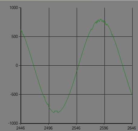
Our customer is evaluating ADC16DV160 on their board, but then they confirmed distortion on digital output as inserted waveform that is converted to analog waveform from digital output of ADC16DV160 by FPGA. They confirmed that the analog signal at input of ADC has no distortion so they think that this distortion may be occurred in ADC. Can you confirm following setting and give your comments?

[Setting]

  • Input Range : 2.0Vpp (It can be also confirmed at 2.4Vpp)
  • Input signal : 1.6Vpp, fixed 1MHz
  • Sampling CLK : 1.4Vpp from Function Generator

[Behavior]

  • The distortion is getting better at higher sampling frequency
  • SFDR is also getting worse at higher sampling frequency
  •  -90dB @ 40Msps
  •  -83dB @ 80Msps
  •  -62dB @ 120Msps
  •  -45dB @ 160Msps

Please let me know if you need more information

Best Regards,

Sonoki / Japan Disty

  • Hello,

    The errors shown in your attached wavefore can be due to the following:

    - Insufficient setup/hold timing at the ADC/FPGA interface causing data capture errors

    - Inadequate or improper capacitive decoupling at the ADC supply pins causing conversion errors inside the ADC

    - Noise on the supplies causing conversion errors inside the ADC.

    - Noisy ground plane causing convserion errors inside the ADC.

    Based on your information, I would first check the decoupling capacitors and their grounding vias and make sure they are all close to the ADC device.

    Regards, Josh

  • Hi Josh-san,

    Thank you for your advice.

    Our customer tried to place the decoupling capacitor on VRPx and VRNx closely, then they could resolve this errors.

    Best Regards,

    Sonoki

  • I have faced same distorsion problem in my design with ADC16DV160. From two channel one channel is pretty clean, where as other channel was distorted. Initialy the distorsion was more. I found that it was DDR data Alignement problem with clock. I tried with once with + clk rising edge and then -clk rising edge. It was mainly because of palcement of DDR FFs inside FPGA at different palces. Finaly the issue is almost settle down with some of from 8 DDR o/ps of ADC "Alignment with + clk" and remaining outputs "Alignment with -clk".
    I my case, both the channel 1 and 2, the decoupling capacitor on VRPx and VRNx are on same distance from pins and One channel was clean whereas other was distorted, this I haven't doubted on this...