This thread has been locked.

If you have a related question, please click the "Ask a related question" button in the top right corner. The newly created question will be automatically linked to this question.

ADC12J4000EVM SCHEMATIC AND THE LMX2581

Other Parts Discussed in Thread: LMX2581, ADC12J4000EVM, LMX2581EVM

e2e,

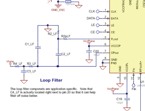
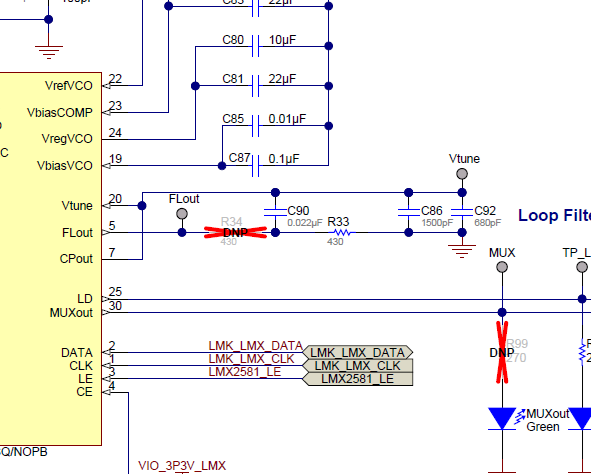
The Ref schematic for the ADC12J4000EVM has the Vtune pin shorted to the CPout for the LMX2581. However, the data sheet shows it a different way. The first two images are from data sheet of the LMX2581 and the last is from the Reference design.

 Which is the proper way? Should we follow the ref schematic or the data sheet? 

Link to LMX2581 datasheet.  

8053.lmx2581.pdf

Link to ADC12J4000EVM Schematic.

1172.ADC12J4000EVM-SCH_E3.pdf

Thanks for your help.

Regards,

John Wiemeyer

  • John,

    The first two images are from the LMX2581 datasheet.  The top colored schematic is actually copied from the LMX2581EVM board instructions, which are also avalable on the web.  The bottom one must befrom the A/D board.

    You are right in looking at the LMX2581 datasheet for this as we just invested a lot of time in this and it was recently updated.   In general, these are all special cases of the LMX2581EVM..   For the b/w picture, this is just the case of R4=C4=0.   For the ADC EVM, this is the case where R3=R4=C3=C4=0.    These 4 components (R3,R4,C3,C4) are good for spurs and supressing the delta sigma modulator noise.  However, if you are using this as some sort of a clock and in integer mode, they might not be necessary.

    If it was my board, I would be inclined to do something that includes the R3 and C3, even if R3=0, because this gives some added flexibility.

    Regards,

    Dean

  • Thanks Dean,

    The customer is using the LMX2581 to clock the ADS12J4000 ADC.  In this specific case is the VTune/CPout circuit in the ASD12J4000EVM schematic correct or should one of hte configurations in the LMX2581 be used?

    Regards,

    John Wiemeyer

  • John,

    Although, the schematic in the ASD12J4000EVM might be "correct"  and is not "broken" and will work, athough I don't know how well optimized it is.   I say this because although I am not familar with the ASD12J4000EVM, but this schematic is one from the original LMX2581 EVM instructions done with our very first silicon before we knew everything about our device, and this was not targeting this particular A/D application.  

    The loop filter can change based on the input and output frequencies, and there are trade-offs between jitter, spurs, phase noise, and lock time.  So there is no such thing as a loop filter that is perfectly optimized for every application, as these requirements differ from application to application.

    For this ADC12J4000EM application, if the PLL is run in integer mode, ten this 2nd order loop filter might be good enough.  However, if the PLL is in fractional mode, then maybe you need the extra pole due to R3_LF and C3_LF.

    I recommend using the datasheet schematic because the ASD12J4000EVM schematic is just a special case of this where R3_LF=0.    If you find that you are happy with this, then great.   However, if you commit yourself to a 2nd order loop filter by removing R3_LF, then you have to re-spin the PCB to add it back.

    So unless you are extremely constrained by board space or the addition of one 0 ohm resistor isa big cost issue, I would use the LMX2581 datasheet configuration because it does not force you into a corner.  For A/D converters, maybe it only cares about noise at far offsets anyways and it makes no difference, but I have not worked enough with A/D converters to know.  It seems that the right thing to do is use the LMX2581 schematic, but choose components that make this equivalent to the ADC12J4000EVM.   But then if you want to tweak it around to optimize it, you have the flexiblity.


    In terms of layout, check out what we did in the EVM instructions.   It is importat to get many components close to the device, so you want to your highest order loop filter capacitor next to the VCO, but it's better to only put this because then you also need the caps for pins 22 and 24 close.  

    Regards,

    Dean

  • Thanks for the additional details Dean!

    Regards,

    John Wiemeyer