This thread has been locked.

If you have a related question, please click the "Ask a related question" button in the top right corner. The newly created question will be automatically linked to this question.

DAC5675A differential clock interface

Other Parts Discussed in Thread: DAC5675A

Hi,

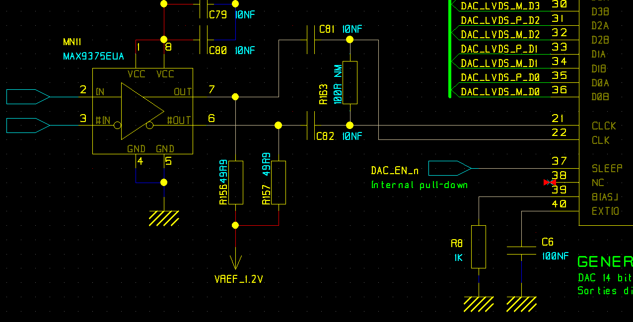
We have designed an interface card with a DAC5675a for RF pulse shaping. The IO card is an FMC card that connects to a Xilinx Spartan 6 FPGA board. I have all of the data bus driven from the FPGA with LVDS25 signals. I also use this (LVDS25) interface to drive the DAC5675A clock input. I am not getting any output from the DAC. Previously I used the DAC5675A eval board interfaced to the  SPARTAN6  ande the clock was single ended and that worked.  I suspect the levels are wrong for the LVDS25 to the clock input. Is there a way to drive the DAC5675A clock input differentially form the LX16 Spartan 6 FPGA? It looks like  I would need to add a resistive divider to drop the lvel down to +2.0V the differential swing of the LVDS is 0.5V so this meets the min differential requirement for the DAC5675A. the board is already laid out, so if I could just change differential types that would be great.

  • Hi,

    I have also added a 0.01 uF cap to the clk input and driven from the SP601 board with a single ended LVCMOS 75 MHz clock. We still have no output. The CLKC input is decoupled to ground with a 0.01 uF cap.

  • Hi Stan,

    Can you provide your schematic? I can send you an e-mail if you don't want to post it here. And what kind of data are you sending to the DAC (constant, sine wave, etc)?

    Make sure SLEEP is pulled low, EXTIO is bypassed to gnd (and not shorted), and BIASJ should have a 960 Ω resistor.

    The clock input should be AC coupled if using a differential signal so that the clock inputs self-bias to 2V.

    Regards,
    Matt Guibord

  • Hi,


    I am designing a similar board with the DAC5675A and I'm having the same issue. I have a ALTERA CYCLONE 5 generating a LVDS clock and I want to use it for clocking the DAC5675A. Is the DAC5675A clock compliant with LVDS voltage swing, or should I use a voltage translator to convert LVDS into LVPECL ? I can see in the DAC5675A datasheet (p6) that the clock differential input voltage range is 0.4Vpp to 0.8Vpp. LVDS voltage swing is 0.4Vpp. Is it to close to the DAC5675A differential voltage range low limit ?


    Also, do I need to terminate the DAC5675A clock inputs (between the AC coupling capacitor and the clock inputs) ? I saw that the clock inputs are self-biased to 2V, but are there also self-terminated ? If no, how should I terminate it ? With a 100 ohms resitance between CLK and CLKP ?

    Thank you for your help,


    Regards,

    Maxime Puech.

  • Hi Maxime,

    DAC5675A has differential LVPECL compatible clock inputs. As you mentioned minimum clock differential input voltage is 0.4Vp-p. As long as your LVDS signal is able to meet the minimum clock input voltage requirements I think it should work.

    Yes, you do need to terminate the DAC5675A clock input with 100ohm resistance between CLK and CLKC. The 100 ohm resister should be placed before the AC coupling capacitors not after.

    Regards,
    Neeraj Gill

  • Hi Neeraj,

    Thank you for your answer.

    I will use a LVDS to LVPECL translator to be safe.

    You said : " The 100 ohm resister should be placed before the AC coupling capacitors not after ". By "before", you mean between the CLK pins and the AC coupling capacitors ? I inserted a part of my schematic above. Is this the clock circuit correct ?

    Regards,

    Maxime Puech.

  • HI Maxime,

    As long as the LVPECL driver see a 100 ohm termination, I think you circuit should work. Remove R156 and R157 and move R163 on the left side of C81 and C82( AC coupling caps).

    Regards,
    Neeraj Gill