A related question is a question created from another question. When the related question is created, it will be automatically linked to the original question.
If you have a related question, please click the "Ask a related question" button in the top right corner. The newly created question will be automatically linked to this question.
I want to use DAC5681Z but i do not know that what is this IC's band width. I want 500MHz BW but I do not know which TI's product can solve my problem, can DAC5681Z?
The DAC5681z can be operated in a 1x bypass mode which will allow you to provide samples at the input of the DAC at 1Gsps, this will allow you up to 500 MHz of Nyquist BW.
I set the register that you said but my problem is about SERDES, recently i worked with DAC5682z.this dac has two 16 bit input channel and a 16 bit ddr output, but this dac has a 1 channel 16bit input and 16 bit ddr output. actually for DAC5681z i have 16 bit input and 32 bit output(16 bit ddr). i don't know how i can set input in SERDES program?!
I'm a little bit confused. The DACs both have a 16 bit LVDS input using a Double Data Rate sample clock. The output of DACs is generally an analog signal per DAC channel.
In the case of the DAC5682z, it is a 16bit DDR input for 2 DAC channel analog outputs. It interleaves the Chan A and B data.
For the DAC5681z it is a 16 bit DDR input for 1 DAC channel analog output. In this case the Data is 2 samples of Chan A interleaved on the DDR clock: A0, A1 then A2 A3, ...
Your interface needs to implement a parallel 16 bit LVDS bus, and depending on the mode you either interleave channel A then B or you interleave 2 samples of channel A per DDR clock edge. This is discussed and a timing diagram is shown in the data sheet.
I have a virtex6 FPGA that i want to give my dds data to this dac. this FPGA can produce a sine data 16 bit in maximum range 500M. So that means i have 16bit data 500M but DAC 5681z needs 32bit 500M (16bit DDR).
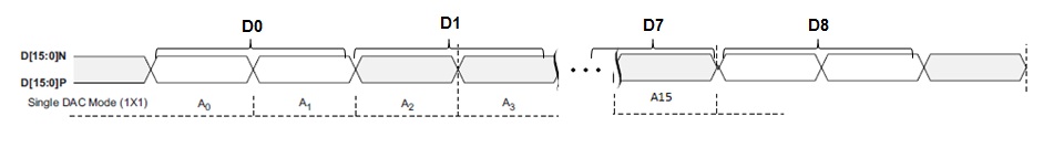
Figure32 in page 34 shows timing diagram of DAC5681z. As you can see, our data is 16bit (A0- A15) while input data of DAC5681z is 16 bit DDR(D0-D15). 16bit DDR =32 bit single, so our sample is 16bit and input of DAC is 32 bit. I show my problem on following picture. In this pic i do not know what data i must set for D8 to D15?!
I think there is some confusion. In the diagram Figure 32 the 16 input bits are labeld as D0..D15, each sample is comprised of the parallel input 16 bits D0..D15. The samples are labeled starting from A0, A1, A2...An+1 (the n-th sample +1 ) . For every DCLK edge a sample of 16 bits Dx is input into the DAC, forming 1 sample of An. Your labeling of D0, D1 ... D8 in your diagram represents 2 samples of A0,A1 and A2, A3...and so on - I'm not sure what you are trying to represent by grouping the samples this way.
So to summarize, the input of the DAC5681z is a 16 bit parallel interface (D0..D16). These 16 bits represent a DAC sample (An). Each edge of the DCLK will clock in a sample for the DAC. The rate at which this DCLK toggles is based on the interpolation and the DAC rate..
The DCLK is a 1/2 datarate clock - this will be a fraction of the output DAC rate based on the interpolation selected. If Interp is bypassed so that the DAC is in 1x mode, the DAC output rate and DAC input datarate are the same - in this case the DCLK is 1/2 of the data rate and 1/2 the dac rate.
If the interpolation is 2x, then the input datarate is 1/2 of the DAC output rate. In this case the DCLK=1/2 datarate= 1/2 (1/2 DAC rate) = 1/4 of the DAC output rate.
I do not know how can i group the samples. i want to program this DAC with FPGA Virtex6 but i thought that my way is true. isn't it?? can you tell me how i can group this clearly?
The interface is 16 bits wide. So you will need to have 16 bit samples. For ever clock edge of the DCLK you will need to provide the 16 bit sample to the 16 bit interface. This is repeated for every rising AND falling edge of the DCLK. There is no serialization involved so the interface is very simple, 16 bits samples every clock edge.
You may need to refer to some DDR (Double Data Rate) clocking schemes which are beyond the support capabilities of this forum. There should be some DDR examples (Not DDR memory, just DDR clocking) from your FPGA vendor.