This thread has been locked.

If you have a related question, please click the "Ask a related question" button in the top right corner. The newly created question will be automatically linked to this question.

DAC8760 output clear

Other Parts Discussed in Thread: DAC8760

Hi,

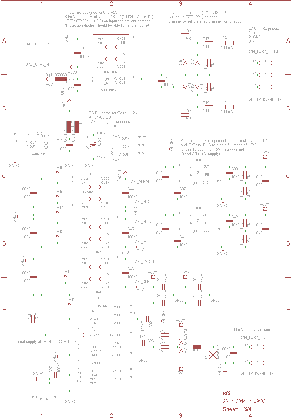
I'm trying to switch the voltage output of the DAC8760 to 0V and back to the previously set voltage by pulsing the CLR and LATCH pins as described in the data sheet on pages 11 (timing) and 36 (DAC CLEAR). The idea is to have a precision voltage source with asynchrounously switchable output.

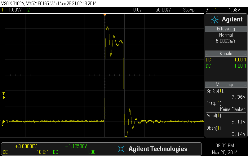
Setting up the DAC output and clearing the output voltage with the CLR pin works fine, but I cannot restore the pre-clear value by "pulsing the LATCH signal". The output stays at 0V. I keep the SCLK pin low - so nothing gets clocked in. As it is I can only restore previous output via MCU by writing to the DAC register again. But this is way too slow to be of any use.

I use a FPGA to translate a digital input signal (hi = output 0V, lo = output voltage) to signals on CLR and LATCH.

To switch the output to 0V I issue a 50ns pulse (hi) on CLR

To restore previous output I pulse LATCH for 83ns (hi).

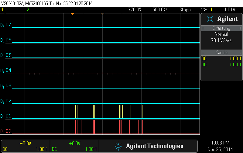
I connected the digital switch input to a pull up and to GND with a wire. If I put the wire in (output should switch on) I get this on LATCH and CLR pins (the port bounces):

D0 = LATCH; D1 = CLR; D2 = SCLK

Zoom on last pair of pulses:

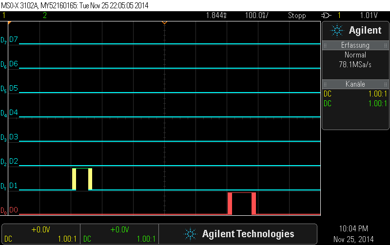
The FSM in the FPGA makes sure (and I checked this) that there is always a CLR pulse between 2 LATCH pulses or a LATCH pulse between 2 CLR pulses. As you can see the last pulse is on LATCH.

As I understood the datasheet this should restore output. Sooo... What did I miss? Why doesn't it work? Any hints and ideas are much appreciated.

  • Arwed,

    Your understanding of this functionality is correct. As a simple sanity check I did some crude manual tests on the EVM using a jumper wire to interface CLR and LATCH with no issues.

    Are you conducting your tests on the EVM board or on a board that you have designed yourself? If it's a board of your own design, can you please share the schematic and layout? In either case, where are the probes placed for you to generate the captures you have shared in this thread?

  • Kevin,

    thanks for verifying the concept. I don't have the EMV board available, unfortunately. I tried single pulses on CLR and LATCH by using the MCU today, but still no luck.

    The schematics for the DAC part are derived from the application circuit in the datasheet.

    DAC schematic and layout:

    The MCU/FPGA side of the ISOs are directly connected to a MCU (ALARM, SDI, SDO and SCK) or FPGA (CLR, LATCH and CTRLP, CTRLN) on other boards with 3.3V. Nothing special there and the longest traces are on this board.

    A LATCH-signal from the MCU can optionally be forwarded by the FPGA. Otherwise LATCH is fully controlled by the FPGA (as is CLR) depending on the state of the CTRLP and CTRLN signals (control input intended to switch the DAC output).

    The probes are placed on the FPGA/MCU side of the ISOs. I'll try to measure the other side later (too bad I missed the opportunity to place some test points on the 1st layout).

  • I now measured CLR and LATCH directly on the DAC and I can confirm: The signals seem to be forwarded correctly.

    A CLR pulse created by the FPGA looks like this:

    (edit: I also posted the schematics and layout a while ago, but got a message that I need confirmation of a moderator. Don't know where this went to... It's obviously not here yet.)

  • After some nerve-wracking trial and error I found the problem myself:

    Looks like you have to clock in a write DAC register command with the output you want restored last thing before you pull the CLR line. ... I understand why it behaves this way, but I'm either blind or there is no word about this in the data sheet. Would have been really nice if this doc would tell you a bit more about how this logic actually works...

    To this point I always switched the output to Hi-Z, wrote the DAC register and switched the output back on by writing to the ctrl register last thing.

  • Arwed,

    Apologies for the delayed response, the end of last week was a US holiday and I was not in office.

    I am glad you found the source of your problem, and there is indeed no indication that this mechanic is required in the datasheet. I will try to get this addressed in a future datasheet revision.

    For others that read this post that may not understand why this is the case:

    If no clocks have been issued between the CLR pulse and LATCH pulse the SPI input shift register will still contain the same data as the previous write. Pulsing the LATCH pin basically "tricks" the device into this behavior because it reloads the word that is contained in the shift register. Assuming the previous write was to the DAC data register you will "restore" the DAC output to the pre-clear value.