Hi,
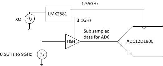
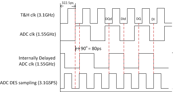
As per my application I have an 12 bit ADC(ADC12D1800) for the RF signal digitalization in the range of 0.5GHz to 9GHz , In order to down convert this in the front end of ADC I have track & hold amplifier. Both T/HA & ADC requires the sampling clock , I planned to provide 3.1GHz sampling clock to THA & 1.55GHz sampling clock to ADC(ADC will be operated in the DES mode). As per the above configuration I want 90 shift between 3.1GHz sampling clock & 1.55GHz clock.I planned to use LMX2581 as a clocking source for ADC as well as TH/A which has two o/p channels. As per my application requirement I want 90degree phase shift between 3.1GHz clock as well as 1.55GHz clock for this I planned to use delay block which is available inside the ADC. I have one query on this ADC12D1800 what is the maximum possible delay we can introduce on the sampling clock on DES mode of operation. Whether the above circuit will work ?
Regards,
Rajesh