


Dear Chris,
I am trying to establish a communication between MSP430 and ADS1258EVM board with more or less success. Based on the guide that you shared I have connected them with Jumper Wires but somehow the result is not that I expected.
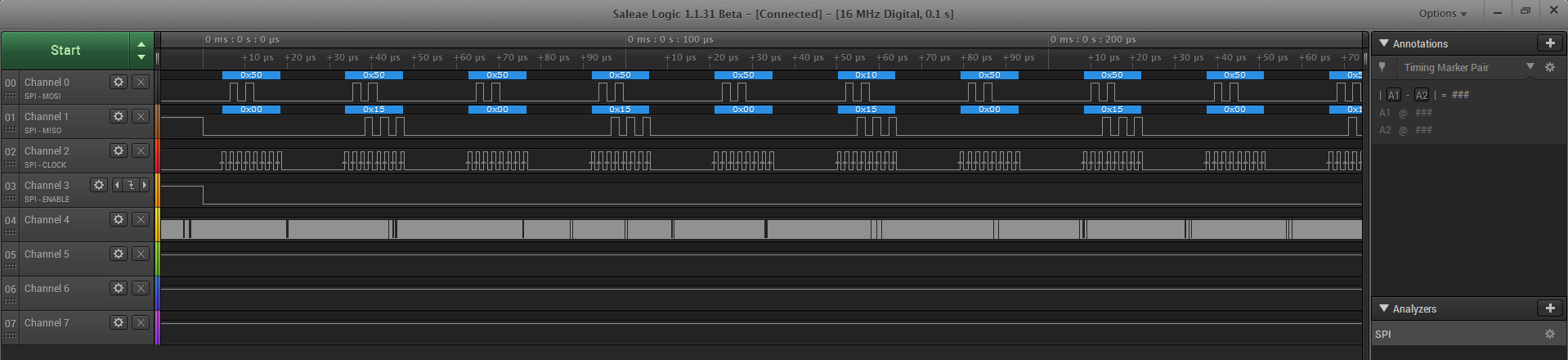
Here is a screenshot of the Saleae:
I am trying to send any command (in this case 01010000 - Read Config0 Registed) and the result is always 0x15. This result is invalid ( the last bit must be 0 all time). Moreover the MOSI values are not always the same... I sense some communication error but I have no clue what to do.
And here is the code that I use:
/* External Clock Pinout
* P5.2/XT2IN
* P5.3/XT2OUT
*
*
* Clock Generation for ADS1268 Master Clock.
* MCLK = SMCK: P2.2
*
*
*
* P3.4 = MISO = <--
* P3.3 = MOSI = -->
* P6.6 = CS = -->
* P2.7 = SCLK = <->
*
* TODO: setDCORef to ExternalChristal for more accure timing? - Ask for help (Why DCO driven clock is so inaccurate in Saleae?
*
* TODO: implement slave reset for ADS!!!
* TODO: Apply Enable or (SS) operation every communication.
* TODO: for(i = 20; i>0; i--); insted of __wait_cycles(cycle_count)
*
* Configure Saleae for Monitoring SPI:
*
* 1) MSB First
* 2) 8bits / transfer
* 3) CPOL = 0
* 4) CPHA = 0
* 5) Enable like is Active Low (Standard)
*/
#include "driverlib.h"
#define SPI_CLK_HZ 500000
uint8_t returnValue = 0x00;
uint8_t transmitData = 0x00, receiveData = 0x00;
void InitGPIO(void);
int InitSPI(void);
void StartSPI(void);
void UseXT2Clock(void);
void UseDCOWithREFO(void);
int main(void) {
WDT_A_hold(WDT_A_BASE);
PMM_setVCore(PMM_CORE_LEVEL_0);
InitGPIO();
//UseXT2Clock();
UseDCOWithREFO();
InitSPI();
StartSPI();
//CPU off, enable interrupts
__bis_SR_register(LPM0_bits + GIE);
}
void StartSPI(){
//USCI_A0 TX buffer ready?
while(!USCI_A_SPI_getInterruptStatus(USCI_A0_BASE,USCI_A_SPI_TRANSMIT_INTERRUPT))
{;}
//Init data values
transmitData = 0x50;
GPIO_setOutputLowOnPin(GPIO_PORT_P6,GPIO_PIN6);
//transmit data to slave
USCI_A_SPI_transmitData(USCI_A0_BASE,transmitData);
// Wait for data complete
//__delay_cycles(100);
//GPIO_setOutputHighOnPin(GPIO_PORT_P6,GPIO_PIN6);
}
int InitSPI(void){
USCI_A_SPI_initMasterParam param = {0};
param.selectClockSource = USCI_A_SPI_CLOCKSOURCE_SMCLK;
param.clockSourceFrequency = UCS_getSMCLK();
param.desiredSpiClock = SPI_CLK_HZ;
param.msbFirst = USCI_A_SPI_MSB_FIRST;
param.clockPhase = USCI_A_SPI_PHASE_DATA_CHANGED_ONFIRST_CAPTURED_ON_NEXT;
param.clockPolarity = USCI_A_SPI_CLOCKPOLARITY_INACTIVITY_LOW;
returnValue = USCI_A_SPI_initMaster(USCI_A0_BASE,¶m);
if(STATUS_FAIL == returnValue){
return 0;
}
//Enable SPI Module
USCI_A_SPI_enable(USCI_A0_BASE);
//Enable Receive Interrupt
USCI_A_SPI_clearInterruptFlag(USCI_A0_BASE,USCI_A_SPI_RECEIVE_INTERRUPT);
USCI_A_SPI_enableInterrupt(USCI_A0_BASE,USCI_A_SPI_RECEIVE_INTERRUPT);
// Wait for a while for Resetting Slave
//__delay_cycles(100);
return 1;
}
void UseXT2Clock(void)
{
GPIO_setAsPeripheralModuleFunctionInputPin(GPIO_PORT_P5,GPIO_PIN2);
GPIO_setAsPeripheralModuleFunctionOutputPin(GPIO_PORT_P5,GPIO_PIN13);
UCS_setExternalClockSource(32000,4000000);
UCS_XT2Start(UCS_XT2DRIVE_4MHZ_8MHZ);
UCS_clockSignalInit(UCS_MCLK ,UCS_XT2CLK_SELECT,UCS_CLOCK_DIVIDER_1);
UCS_clockSignalInit(UCS_SMCLK ,UCS_XT2CLK_SELECT,UCS_CLOCK_DIVIDER_1);
}
void UseDCOWithREFO(void){
// Set VCore for 16MHz
PMM_setVCore(PMM_CORE_LEVEL_2);
//Set DCO FLL reference = REFO
UCS_clockSignalInit(UCS_FLLREF,UCS_REFOCLK_SELECT,UCS_CLOCK_DIVIDER_1);
// Ratio = MCLK_FREQ_KHZ / FFL_REF ~ 4000 / 32.768 = 122.07
UCS_initFLLSettle(8000,244);
}
void InitGPIO(void){
// LED
GPIO_setAsOutputPin(GPIO_PORT_P1,GPIO_PIN0);
// P2.2 for SMCK
GPIO_setAsPeripheralModuleFunctionOutputPin(GPIO_PORT_P2,GPIO_PIN2);
// Configure for SPI
// P3.4 as MISO
GPIO_setAsPeripheralModuleFunctionInputPin(GPIO_PORT_P3,GPIO_PIN4);
// P3.3 as MOSI
GPIO_setAsPeripheralModuleFunctionOutputPin(GPIO_PORT_P3,GPIO_PIN3);
// P2.7 as SCLK
GPIO_setAsPeripheralModuleFunctionOutputPin(GPIO_PORT_P2,GPIO_PIN7);
// P6.6 Chip select
GPIO_setAsOutputPin(GPIO_PORT_P6,GPIO_PIN6);
// Set SS or Enable to High
GPIO_setOutputHighOnPin(GPIO_PORT_P6,GPIO_PIN6);
}
#if defined(__TI_COMPILER_VERSION__) || defined(__IAR_SYSTEMS_ICC__)
#pragma vector=USCI_A0_VECTOR
__interrupt
#elif defined(__GNUC__)
__attribute__((interrupt(USCI_A0_VECTOR)))
#endif
void USCI_A0_ISR(void)
{
switch(__even_in_range(UCA0IV,4))
{
//Vector 2 - RXIFG - Check if any response arrived from slave side
case 2:
//USCI_A0 TX buffer ready? check if all characters are sent
while(!USCI_A_SPI_getInterruptStatus(USCI_A0_BASE,USCI_A_SPI_TRANSMIT_INTERRUPT))
{;}
// no need to wait here, slave data arrives ontime.
receiveData = USCI_A_SPI_receiveData(USCI_A0_BASE);
//Increment data
//transmitData++;
//Send next value
USCI_A_SPI_transmitData(USCI_A0_BASE,transmitData);
//wait between transmissions for slave to process information
//__delay_cycles(40);
break;
case 4: break; // Vector 4 - TXIFG
default: break;
}
}
Here is another screenshot about ID Register: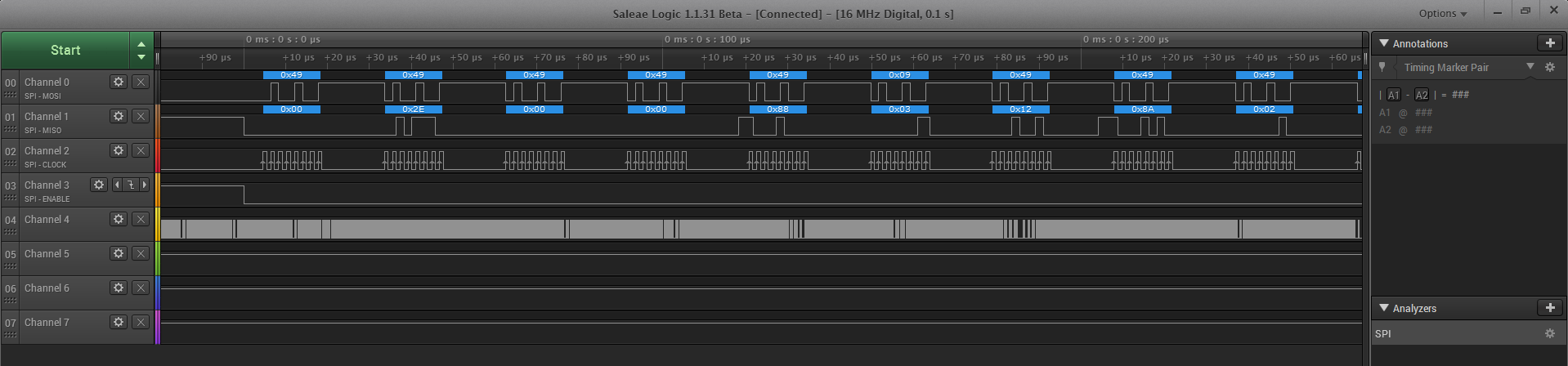
Looking forward your kind reply,

