This thread has been locked.

If you have a related question, please click the "Ask a related question" button in the top right corner. The newly created question will be automatically linked to this question.

SPI Communication problem with ADS1248 IPW

Other Parts Discussed in Thread: ADS1248

Hello

I'm using an ADS1248

/RESET is set to High

CLK is set to Low

START is set to high always.

I try to write a register and then immediately read it, but MISO stay always low then read data is always 0!

I send command SPI 0x40 0x00 0x07 to write 1 register MUX0 (Addr 0x0) value 7 (MUX_SN = 7, MUX_SP = 0)

Then to read I send  command SPI 0x20 0x00 0x07 to read 1 register MUX0 (Addr 0x0). Last byte is a dummy to read returned value.

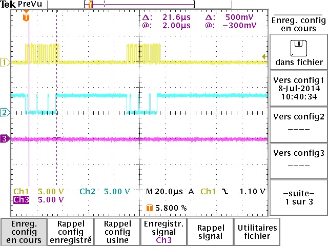
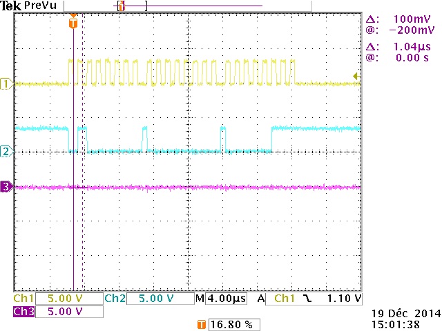
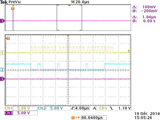
Please find scope trace:

Yellow = SCLK, Blue = MOSI, Red = MISO:

Global.Jpg:  We can see the read and write sequence.

Write.jpg: Zoom on Write sequence

Read.jpg: Zoom on Read Sequence.

Please, Have you an idea why returned value is always 0?

PS I try to send a SPI CMD RESET and then waiting 600ms and then Write/Read. But this no change the result.

Global:

Write:

Read:

Thanks

  • PS: CD pin goes low long time before clock oscillation..
  • A GIR,


    In general, your waveforms look correct. This version of SPI uses SCLK dwelling low, while DIN is clocked in on the falling edge of SCLK. The only thing that might be off would be that in your setup, the DIN line dwells high, but I don't think that would be a problem.

    Just to review (and make sure you verify these):
    START should be high
    /RESET should be high
    /CS should be low for communication (low through the entire communication, not just for individual bytes). In your last post, you mention CD and I think you meant CS.

    One of the first things that I would look at would be the /DRDY line. When first turned on, the device will automatically start converting. Check the /DRDY line for a pulse at the data rate (it will be a narrow pulse to indicate that the device is making conversions). If you can't see this, the device is either off, shutdown, in reset, or there's just no power going to it.

    If you see /DRDY, then start clocking in SCLKs. If the /DRDY goes high in response, then you know that the SCLKs are reaching the device. After that try changing data rates by writing to the appropriate register. If you can see the data rates change with the period of the SCLK, then you know the DIN pulses are reaching the device. Then you're left with the DOUT line as the culprit.

    Let me know if you get further debugging your board. Post back when you can.


    Joseph Wu
  • Hi,

    I made all verification and all seems Ok,

    I change my board with another, and then I have a correct response now when I red Register!...

    Then I read Offset register, I get 0x0

    I read FullScall register, I get 0x400900, this seem a correct value.

    But now, I try to get conversion result, but value change always!

    Bellow my hardware which allow to measure with a PT1000. (used in two wire)

    Then for my test, I have:

    ANI0 -> R(330Ohm  + 1690) -> PT1000 (1K fixed for test) -> R(330Ohm+ 1690) -> ANI7

    ANI7 is directly linked to REFP0. And then this is linked with a Rbias resistance of 11KOhms.

    REFN0 is link to AVSS.

    Then SPI sequence is following:

    -Send MUX0 set to 0x07 (PosInput = ANI0, Neg = ANI7) (CS goes low and then goes High)

    -Send MUX1 set to 0x00 (Internal Osc, VRef internal OFF, RefSel = REF0, MUXCAL = 0 for normal operation) (CS goes low and then goes High)

    -Send SYS0 set to 0x60 (PGA = 64, DOR = 5SPS) (CS goes low and then goes High)

    -Send SYS0 set to 0x60 (PGA = 64, DOR = 5SPS) (CS goes low and then goes High)

    -Send IDAC1 set to 0x0C (First DAC to ANI0, Second DAC disconnected) (CS goes low and then goes High)

    -Send IDAC0 set to 0x02 (DRDY Only DOUT, Current = 100µA) (CS goes low and then goes High)

    Then DRDY pin goes High after the first SPI communication and then goes low about 300ms after.

    Then I read data, DRDY goes High and then Low after 200ms .

    Then I Wait DRDY is Low to start a read data, this make DRDY goes High etc...

    But value read each time is very different!

  • NB: when PT1000 is not connected (My Stub Resistance of 1K), the resukt of conversion returned is always 0x7FFFFF)

  • And then with the scope, I read ANI0 ANI7/REFP0, these pine stay always to 0V..
    It seem the REF0/ANI7 should be during the sample to (100µA * 11K) = 1.1V...

    When I read all registers in the same SPI CS sequence, I read following (in Hexa): {0x07, 0, 0, 60, 0, 0, 0, 0 , A, 40, 92, 0C, 0, 0 , 0}

    This seem Correct

  • Hi A GIR,

    if I understand your setup correct, then all you need to change is to turn the internal voltage reference on, VREFCON=01.
    The internal reference needs to be turned on in order to use the excitation current sources.
    However you would use the external reference for the measurement, REFLSELT=00.

    Just to be on the save side you may want to post your schematic portion of the ADS1248 as well.

    Regards,
  • Hi,

    I seen fo VREFCON.
    THen after turn on it, ADC work correctly now.

    Thank you