Dear Chris,
First of all, I would like to wish you a Happy new year and thank you for your support in 2014! :) Don't worry I will have many more question in 2015.
I am using ADS1258EVM without MMB0 based on the wiki guide that you shared. It works very well, thank you for the nice work. Right now, the Vref switches are in left position (0V-5V) but I would like to control the Vref via DAC. Before I start this work, I have some questions:
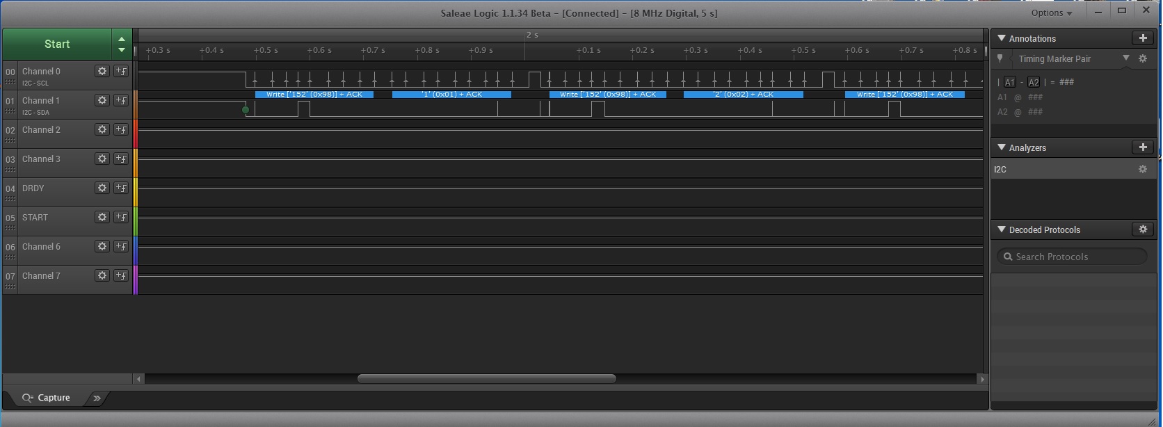
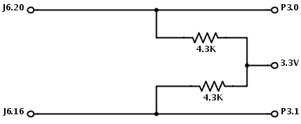
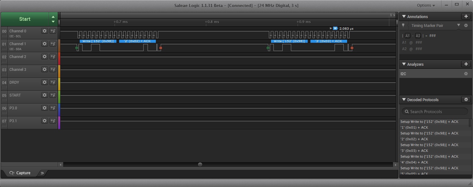
- Is it possible to fully control ADS Vref with DAC8571 through pins located on J6A?
- Do you have any recommendation for the I2C implementation? Address: 1001100 | Set S1 and S2 to Center position
- On the EVM guide: "The output of the DAC is multiplied by two, giving a range of approx. 0V to 5V." Could you explain this behavior ?
Thank you in advance,