This thread has been locked.

If you have a related question, please click the "Ask a related question" button in the top right corner. The newly created question will be automatically linked to this question.

ADS1148: correct communication sequence?

Other Parts Discussed in Thread: ADS1148

Hi,

I'm working with a ADS1148 with a PT1000 connencted in order to get a temperature information. I'm still not abe to get a result that could have a sense.

Now I am do the following steps:

  • Initialize SPI communication
  • Sent RESET command to the ADS1148
  • Send Self Calibration Command
  • Wait for DRDY going low
  • Write the 15 configuration registers
  • Delay
  • Pull the START pin high to start the conversion
  • Send RDATAC command (Read Data Continuously)
  • Wait for DRDY going low

  • Send NOP command (0xFF)
  • Read 1 byte from SPI
  • Send NOP command (0xFF)
  • Read 1 byte from SPI

(The CS pin is obviously low when a SPI communication is in course.)

Can anyone tell me if the steps above are not correct?

Is there a reason because I'm not able to read out a valid information from the conversion? Perhaps I forgot some steps?

Thank you in advance,

best regards

Andrea S

  • Andrea,

    I would change the communication order a little.

    • Initialize the SPI communication (I'm not sure what your doing for this, but it might be necessary for the micro you are using).
    • Send a RESET command
    • Write the configuration registers
    • Send Self Calibration command (do this after the configuration registers are written)
    • Toggle START (I would have initialized everything with START as high). Here you can toggle it low and high to initiate a conversion.
    • Wait for DRDY to go low. The RDATAC mode should be default so you don't need to go into that mode.

    To read the data:

    • Pull /CS low
    • Read two bytes from SPI
    • Return /CS high (CS is low through the entire communication transaction, not for each byte).

    If there are still problems, check two things. First, make sure that the SCLK dwells low and the data is clocked out on the falling edge of SCLK. Second, try reading back the configuration register that you've written. If all else fails, use an oscilloscope and send a scope shot of the communication transaction, including DOUT, SCLK, DRDY and CS. Also, send the data you are receiving.

    Joseph Wu

  • Joseph,

    many thanks for your answer.

    I changed my code according with your suggenstions.

    Now, I do the following steps:

    • Initialize the SPI communication with the clock High when communication is Idle (data clocking at the falling edge)
    • hardware reset of the device by putting low the /RESET pin for about 6us
    • pull High the START pin
    • Send the RESET Command (0x06) to the device
    • Write the configuration registers: in this case, i want to measure the external VREF between REFP0 and REFN0 pins
      • /CS low
      • first, I send the 2 WREG bytes
      • then, I send the 15 byte of the configuration registers
      • /CS high
    • Send the SELFOCAL command (0x62)
    • 20us delay
    • Toggle START pin:
      • START low
      • 10us delay
      • START high
    • while cycle to wait the DRDY pin going low
    • /CS low
    • Send through SPI 0xFF (NOP command)
    • SPI receive byte function and save the byte into a variable
    • Send through SPI 0xFF (NOP command)
    • SPI receive byte function and save the byte into a variable
    • /CS high

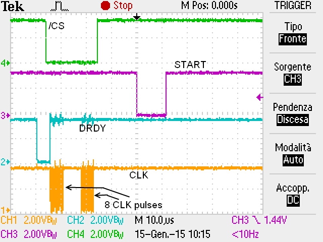
    Here there is the behaviour  of the CLK, DRDY, STARD and CS signals:

    Looking the shot, it seems that the START pin is toggled BEFORE the communication, but I think it is from the following cycle of operations . I can't show in the same shot the propper START pin going low and high.

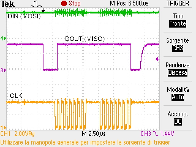
    Below I show the DIN and DOUT in respect with the CLK


    On the DOUT pin I can see something, perhaps the NOP bytes, but on the DIN pin I'm not able to see anything..

    May I forgot some passages or did any mistakes?

    Thanks again,

    Andrea S

  • Andrea,

    Make sure the SCLK dwells low (that SCLK starts low and clocks up for a pulse). It is not set up that way according to the scope photo.

    It might affect the data clocking out and clocking in register values.

    Joseph Wu

  • Joseph,

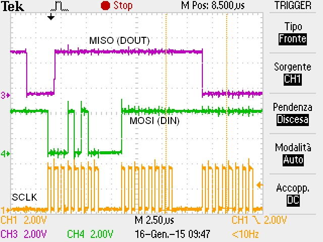
    1. yes, you are right about the behaviour of the SCLK when idle: I modified the SPI initialization, and the new scope photo of the communication is shown here:

    2. but now I have a doubt: I'm trying to measure an external VREF (about 1,5V) between REFP0 and REFN0 of the ADS1148; in order to write the configuration registers, I write the MUX1, IDAC0 and IDAC1 registers, at the address 02h, 0Ah and 0Bh rispectively. To do this, I send the WREG command and after that the single byte through SPI, and repeat it for three times, in this way:

    /CS is low here
    ucArrayToSend[0] = 0x42;
    ucArrayToSend[1] = 0x00;
    ucArrayToSend[2]  = 0x35;	// 00110101	(MUX1 - ADDRESS 02h)
    
    for (i = 0; i < 3; i++)
     ADS_1148_SendByte(ucArrayToSend[i]);  // this is the SPI send byte function
    //--------------------------------------------------------------------------
    ucArrayToSend[0] = 0x4A;
    ucArrayToSend[1] = 0x00;
    ucArrayToSend[2] = 0x01;	// 00000010 (IDAC0 - ADDRESS 0Ah)  IDAC1=50uA
    for (i = 0; i < 3; i++)
    	ADS_1148_SendByte(ucArrayToSend[i]);  // this is the SPI send byte function
    //--------------------------------------------------------------------------
    ucArrayToSend[0] = 0x4B;
    ucArrayToSend[1] = 0x00;
    ucArrayToSend[2] = 0x3F;	// 00111111 (IDAC1 - ADDRESS 0Bh) //IDAC1 connected to AIN3, IDAC2 disabled.
    for (i = 0; i < 3; i++)
    	ADS_1148_SendByte(ucArrayToSend[i]);  // this is the SPI send byte function
    //--------------------------------------------------------------------------
    /CS go high here

    After that, I want to start the communication (toggle START pin, wait for DRDY to go low, send RDATAC command) and receive the measured VREF voltage an the REFP0-REFN0 pins, but if I trigger the oscilloscope on the MISO signal (DOUT), I can see data that don't make sense. My VREF (REFP0-REFN0) is about 1,5V (measured with a multimeter), but the reading of the oscilloscope doesn't match with it. Perhaps the configuration is wrong? Have I to configure other registers?

    my steps in this step are:

    • pull the START pin low and high
    • while cycle to wait the DRDY to go low
    • /CS low
    • send RDATAC command through SPI
    • send 0xFF through SPI
    • receive a byte from SPI
    • send 0xFF through SPI
    • receive a byte from SPI

    Could anyone tell me what I'm doing wrong?

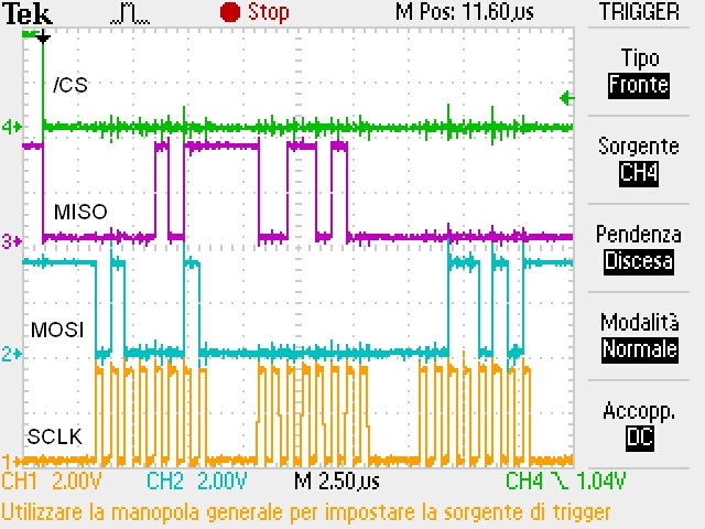
    Here is the scope photo of the communication:

    Many thanks!

  • Andrea,


    Thanks for the scope shot of the communication. It was important to get the SCLK in the right format. For the first shot, it looks like 14h followed by two NOPs which would be RDATAC. In your system, I don't think you need to issue that command, because RDATAC is the default mode of getting data. It doesn't hurt to leave it in, but it's not necessary. Once the /DRDY goes low, you can simply send the NOPs to get the data value back. The data is ready to be clocked out of the DOUT register.

    Looking at the code you provided, it looks correct for what you are doing. The last scope photo shows the sequence of 42h 00h 35h, for setting the single byte of the MUX1 register. That should set the internal reference always on, the onboard reference selected, and a measurement of the external REF0/4 as mentioned in Table 17 in the datasheet. Measure REFOUT to GND to make sure that the external reference is correctly at 2.048V

    With that setting, you should have an output data of:

    ((1.5/4)/2.048V)*2^15 codes for the output or about 6000d, or about 1770h.

    If you do not get this value, what value do you get?

    One thing to check would be to read back the data that you've written in the register. That way, you know that the device has taken your commands.

    Another thing to try would be to put the MUXCAL bits back to 000 in normal operation and put the 1.5V on the proper input to measure that (perhaps AIN0 and AIN1 as the default). Let me know what data you are reading out in either case. Are there any other registers that you are using (VBIAS, SYS0, etc.)?

    Here are a couple of other questions:
    Are you using the on-board oscillator? If you are or if you are using a 4.096MHz clock, Is SCLK a frequency lower than 2MHz? Note that the min SCLK period is 500ns. I think it is fine, based on the scope shots you've provided.

    Also, once you receive the /DRDY low indicating complete conversion, you should immediately clock out the data. If clocking out the data is delayed and is too slow, then there is a chance that the ADC completes another conversion, if that happens, the DOUT register is updated in the middle of clocking out the last conversion, and the output data is corrupted. Can you check to see if this could happen in your system?


    Joseph Wu
  • Joseph,

    Thank you for your exhaustive answer: now I succeded in measuring the VREF between REFP0 and REFN0. I did the steps thant i described in my last post, but with the following differences:

    • I send the RDATA command instead of RDATC command
    • I wite the configuration registers every loop cycle: it seems it is not sufficient to write them one time at the start. Could you tell me why? It is the expected behaviour?

    As you suggested, I will now try to change the configurations, and try to measure a signal connected to the AIN0 and AIN1 (that is my main purpouse), disabling the internal reference and using the previously measured VREFas voltage reference.

    Thanks again!

    Andrea

  • Joseph,

    as I wrote in my last post, I tryied to measure from the AIN0-AIN1 input (I have a resistor connected simulating a PT1000 sensor). I followed the same steps as I did previously with the VREF (REFP0-REFN0) measurement, but I obtain values from the conversion that doesn't have any sense.

    I'm writing the configuration registers as follows:

    (MUX0 - ADDRESS 00h)  <--  11000001      My measure is between AIN0 and AIN1

    (MUX1 - ADDRESS 02h)  <--  00100000     I use internal oscillator

    (SYS0 - ADDRESS 03h)  <--  00100000     I set the PGA to 4  and the data rate to 5SPS

    (IDAC0 - ADDRESS 0Ah)  <--  00000010   The IDAC is set to 100uA

    (IDAC1 - ADDRESS 0Bh)  <--  00111111    The IDAC output is AIN3

    At this point, I think there should be something wrong in configuration shown, but I don't really understand what. Can you see something that doesn't match with my measure on the AIN0-AIN1 input?

    Thanks again,

    Andrea

  • Andrea,


    I'm not sure of the implementation of your circuit so it's harder to know what is wrong. You may have to post a schematic if you are able.

    First, what value are you getting and what are you expecting? What are the values of the resistor and the reference resistor? Have you measured the input directly with a multimeter? Have you measured the reference? What values are you getting?

    If you have the RTD connected from AIN0 to AIN1, why are you driving AIN3?

    Go through these questions and respond this post with a few answers. I'm sure that we can solve your problem.


    Joseph Wu
  • Joseph,

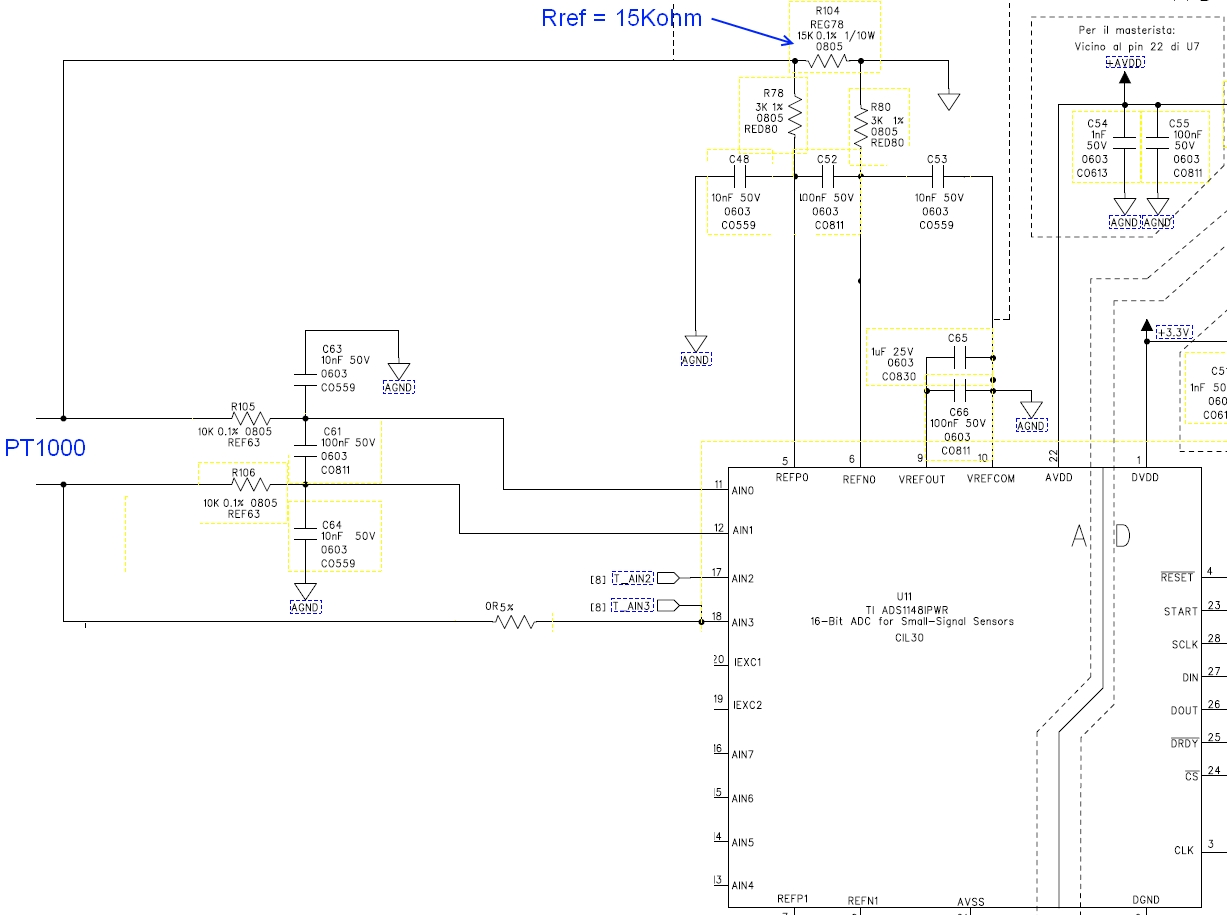
    this is my schematic:

    • The reference resistor is 15Kohm, I selected an IDAC value of 100uA, so the Vref (REFP0-REFN0) should be about 1500mV (and I can read it correctly with a multimeter).
    • I thought the IDAC current should be routed to AIN3 because, looking at the schematic, that current flows through the PT1000 and generate a voltage differences that I can measure between AIN0 and AIN1. Is it correct?
    • For example, a resistance of 1,7Kohm is connected to the inputs, simulating a PT1000 value. Measuring the voltage at the inputs with a multimeter, I can read a voltage of 160 or 170 mV. Running the program, the ADS1148 reads a value of about 0xC6A3 (50850d). I think it is not correct, because this value corresponds to a voltage of: Vin=Vread*VREF/(PGA*32767) = 50850*1500/(4*32767)=581mV , that is different from 170mV I measure on the board. Perhaps there is any error in the formula I used?

  • Andrea,


    Based on the way you have it set up, it is ok that the IDAC is sourced from AIN3. However, notice that the current will make the AIN1 node higher than AIN0. If you have the default measurement of AIN0 as positive and AIN1 as negative, then the voltage you read will be a negative value.

    Note that a negative value is represented in twos complement notation. In your reading, you get C6A3h which is -14685d. Note the data format explained on page 30 of the datasheet.

    Using this, you can calculate the measured value (ADC data/2^15)*(VREF/PGA). Note that full scale is -VREF/PGA to +VREF/PGA to get 2^16 bits. (and 0V to +VREF/PGA for half the full scale to get 2^15 bits).

    Measured value = (-14685/2^15)*(1.5V/4) = -0.168V.


    Joseph Wu

  • Joseph,

    you are right! I was measuring a negative voltage at the input! I changed the MUX0 register setting the AIN0 as positive input and the AIN1 the negative one, and now the value the ADS1148 reads is a positive and right one. Thanks!

    Just another last question. As I mentioned before, I am now able to measure the potential difference on my PT1000, and it is almost the same as the one I measure with a multimeter on the board (OK). Since I would like to measure a temperature, I calculate the resistance of the PT1000 as

    R(PT1000) = (AIN1-AIN0)*100uA  (I selected a 100uA IDAC),

    but I obtain a resistance value that is not really the same as the one measured on the PT1000:

    At ambient temperature:

    • R(PT1000) measured with a multimeter: 1096 ohm
    • R(PT1000) calculated by the ADS1148: 1050 ohm

    Since the (AIN1-AIN0) is well measured from the device, I think that there would be an error in the current, perhaps it is not exactly 100uA. Can it be possible? Which can be a possible cause of this error?

    I would like to solve this problem, because in my system it means some °C celsius of difference.

    Do you have any suggestion or idea?

    Many Thanks,

    Andrea

  • Andrea,


    There may be error in voltage but it should be exact in resistance. In the way you have the ADC set up, the measurement is ratiometric. While the current may have some absolute error, all of the current is flowing through the RTD and reference resistor. That means the measurement from the ADC divided by the 7FFFh, will be the exact ratio between RTD resistance divided by the reference resistor value. In the end you don't need to know the reference voltage value exactly, you only need to know the reference resistor value exactly.

    There are two things become important. First you need to have a reference resistor that is very accurate. This may determine the accuracy of your system. Second, there should not be any leakage paths for the IDAC current to go and the current should only go through the RTD and the reference resistor. There may be some input impedance which may alter the apparent resistance with the input and the reference, but that should be minor and you should be able to calculate it.

    What is the accuracy of the reference resistor that you are using?


    Joseph Wu
  • Joseph,

    the reference resistor I am using is a 15Kohm 0,1%, so I think the accuracy should be enough.

    While I was reading your kind answer I was thinking about this:

    Assuming the 100uA (IDAC current) is not so accurate, I can calculate it in the meantime I am measuring the VREF:

    IDAC_current(REAL) = VREF(calculated)/ReferenceResistor.
    Perhaps I would obtain a value a bit different from 100uA.

    In this way, I can use the calculated value of the current (instead of assuming it is exactly 100uA) in order to calculate the RTD resistance, that is my goal.

    Does it have any sense in your opinion? May it works?
    Thanks!

    Andrea
  • Andrea,


    I'm not sure exactly what you want to do based on your explanation. If you want to measure the VREF based on the IDAC current on the reference resistor, you could do it that way, but there may be shifts in the IDAC current over temperature. After that the VREF would change and you'd have errors again.

    The method I describe is very common and the error in the reference resistor should be the primary error. This way, you don't need to have an accuracy measurement for the reference voltage or the IDAC current.


    Joseph Wu