This thread has been locked.

If you have a related question, please click the "Ask a related question" button in the top right corner. The newly created question will be automatically linked to this question.

ADS1148 reads negative

Other Parts Discussed in Thread: ADS1148

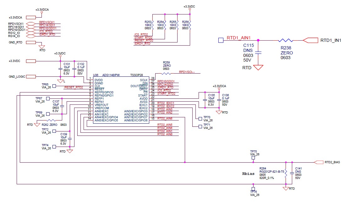
We are using ADS1148, 2 wire configuration. We are using 1k pot to simulate the RTD.

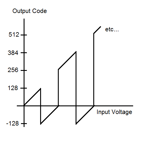
Our issue is: We are getting good readings for 1-100 ohm. Above 100 ohms, we are are getting negative values (65555). If we keep increasing the resistance, above 300 we are getting good readings. What would be the possible cause?

Thank you.

  • Amar,


    Could you please post a basic schematic (if you are willing). I'd like to see how you have it set up. Are you using some sort of hardware compensation (resistor to null the RTD value).

    I'd like to know what your IDAC currents are, where they are going, and what your reference resistance is.

    Also, I'd like you to take measurements of the reference and the inputs with a multimeter (record the voltages), and then record the data value in hex or decimal. Put those values into a table and post back so I can read through it.

    At this point, there's not much information to help you debug the circuit.


    Joseph Wu
  • Joesph,

    I am working on the same project as Amar. I can get you all the info you requested, but before I do so I wanted to describe the issue a little better.

    To me it seems we have some data shaping issue with the chip, but first here is a general description of our setup.

    We are using a 1k pot to simulate an RTD, in a 2-wire setup. Using Internal 2.048V ref, exciting AIN5 (positive channel) and reading it to AIN7 (negaitve channel). We have the pot between AIN5 and AIN7. AIN7 sits around 1.2V and AIN5 goes from 1.2V to ~2.5V as we adjust the pot.

    Anyways we get what seems like good reads when the read range is from 0-127, 256-383, etc. And the read goes negative from 128-255, etc.

    So when bit7 of the data output should high, the entire MSB of the data output also goes high, giving us the negative read pattern I described.

    I have reproduced this behavior with various gain and excitation settings, which I think further shows that this is some data shaping issue with the chip and not an issue with the hardware setup.

    All of our offset registers are defaulted, and I don't think the offsets are capable of producing the data shaping that we are seeing.

    Let me know your thoughts and if you would still like to see some schematics, and perhaps a table of voltages and the associated data outputs.

    Thanks,

    Devon Mahn
  • Devon,


    Both the schematics and the table of voltages (both the input and reference) and data values will be helpful. I would have thought that you would make a ratiometric measurement using the current DACs and a reference resistor, so I'd like to see a schematic (even a partial schematic).

    I was pretty sure the offset and gain registers would be default. However, let me know what gain and data rate you are using (and any other configuration settings that you have made.


    Joseph Wu
  • SN

    Resistance (Ohm)

    Reference & Input Voltage (V)

    Data Value

    1

    0

    0

    0018

    2

    100

    0.14

    65491

    3

    200

    0.29

    65426

    4

    300

    0.44

    5971

    5

    400

    0.58

    7959

    6

    500

    0.73

    65497

    7

    600

    0.88

    65435

    8

    700

    1.02

    13915

    9

    800

    1.15

    15901

    10

    900

    1.27

    65535

    11

    1000

    1.38

    655535

    Reference resistance is 820ohm. I am supplying  IDAC current of 1500uA on each positive input while switching. My Positive inputs are AIN1 to AIN6 and AIN7 is negative input. Reference voltage across the REF0 is 1.21V.

    Thanks.

  • Joe,


    Here's the schematic for our RTD circuit. Taking the data for a voltage vs output table would take some time, so I figured I would start of with just the schematic.

    Other settings I may have missed: 2ksps, usually a Gain of 1, and excitation of 1.5mA, but we have reproduced this behavior across various Gain and Excitation settings.


    To simulate an RTD sensor, we wired a 1kPot between AIN5 and AIN7/REFP0.

    -Devon

  • Joseph,

    I wanted to add some further input to Amar Description again. We actually do get some bad reads into 0-100 range (my setup I can more finely adjust the resistance).

    Again I want to stress that I think there is some data shaping issue, as the output results are too perfect.

    If I start the pot at zero resitance I get a good read of zero. As I slowly increase the resistance on the pot, I see the output climb linearly. Once I pass the output threshold of 127, i get a negative value starting at (65535-128). If i continue to incearse resistance, the output climbs from (65535-128) to 65535, where it then jumps back to 256 as a good read. This pattern repeats itself across all the data I and Amar have collected. Where if the bit7 is high, the entire MSB of the data output is also high. if you check the binary of all of Amar's good data reads, you will see bit 7 is low.

    I have been able to reproduce this bit7 issue using various Gain, Excitation, Vref settings, and ads1148 chips. To me this issue is too perfectly correlated with the data output to think it would have to do with a circuit setup problem and the data looks exactly as it should when bit7 is not supposed to be high.

    Thanks for all the help!

    -Devon
  • Devon and Amar,


    I'm still looking at the schematic, but do you have an oscilloscope to show the data transaction? I'd want to see the /CS, SCLK, DIN, and DOUT for a data read of a good and bad case.

    Also, what is your SCLK rate?


    Joseph Wu
  • Joseph,

    We are running a 4MHz SCLK. I couldn't find a CLK specification on the data sheet, and I have been able to successfully read and write registers so I assume I was in the acceptable range.

    I would be happy to take some nice capture of the SPI BUS for you. I'll start working on those for you tomorrow morning. Hopefully you can have a chance to finish looking over the schematic as then as well, and alarm us of any circuit issues before I spend an hour or two capturing the SPI BUS :).


    Also I have attached I hand drawn schematic of how I have my 1kpot hooked up (Amar and I are on two different set-ups).02191501.PDF

    Thanks again for all the help. If I have not heard any bad news about our circuitry by tomorrow morning I'll start working on some SPI Bus captures (as well as associated voltages).

    -Devon Mahn

  • Devon and Amar,

    Just to be clear, is this what you are seeing?


    After that, the pattern repeats all the way up to full scale (output code=32767)? How do you extract the data? Do you do any manipulation in the read to account for 2s complement notation?

    At this point, I'm assuming that you are looking at one channel (I'm going with Devon's AIN5 to AIN7), then sourcing current from AIN5 to sink through Rbias, which is connected to AIN7. Assuming that there are no leakage currents, then all of the current (1.5mA) through the pot should also go through Rbias.

    With the IDAC current at 1.5mA, voltage across the Rbias should always be 1.23V. For the pot, it should go from 0V to 1.5V, but the data should overrange at the same 1.23V when the pot resistance is 820Ohms, same as Rbias. I assume that you're not changing channels and that you're reading the inputs based on the input value and not through the sample and hold devices on the front end.

    Let me know if I've missed anything in the explanation.

    I'd definitely look to getting the scope shots I asked for earlier. It might shed some more light onto the problem.

    Joseph Wu

  • Devon,


    If fclk is 4.096MHz, then the max SCLK is 2MHz. I'd slow it down to see if it helps.


    Joseph Wu
  • Joseph,

    I tried running a 1MHz SCLK, and the behavior remained the same (both to my relief and dismay).

    Your function graph shows what we are seeing with data output.

    Data extraction is pretty simple. We grab a byte of data from the SPI Bus at a time, transferring the two bytes into a signed short (MSB gets a byte shift). I have verified my reads with the SPI DOUT a few days ago, and they seemed accurate. We will be able to review that again when I get you some SPI Bus captures though.

    Everything you said seems accurate. I'm not changing channels. Taking a differential between AIN5 & AIN7, gives us an effective range of 0-1.5V across the pots range. We should then have overrange when or Vin passes 1.23V, which Amar should have hit, but based on his data when he overranges he is always reading 65535 (supports my 7bit data shaping theory).

    So it sounds like we are all on the same page and you don't have any glaring concerns that would explain our issue. I'll go ahead and plan on getting those SPI captures first thing tomorrow morning.

    Thanks again for your help and responsiveness! We really appreciate it!

    -Devon
  • Joseph,


    I was able to discover our issue after I more closely analyzed to SPI Bus.


    To extract data reads we were us a READ command, and then collecting the next two bytes by sending NOPs. Since the ads1148 defaults to continuous data mode, it was clocking out the MSB of the data read while we sent the READ command.


    Here' s a a scope shot (CLK = yellow, CS = Green, DOUT = Purple). This shot captures right when I passed over the 127 DOUT threshold.  It seems when the DOUT clocks out the data MSB the first time, it preemptively sets bit7 of the LSB. Then we we try to read the MSB after out READ command, we latch on DOUT before we should, getting a 1 for the high byte of the read. Folow two's compliment rules and that explains our negative reads.


    We are most likely running an innapropriate SPI Mode, and need to latch datha on CLK low, not CLK high. I guess it would be nice if the SPI Mode as well as rate was explicitly stated in the datasheet. Either way I was able to solve this by just reading in the data without first sending a READ command.

    Thanks again for all the help!


    -Devon Mahn

  • Devon,

    It looks like you're on your way to getting some good data. I would like to point out a couple things. Most of the communication specs are shown in the tables and diagrams on page 12 of the datasheet. Based on the scope shot, you'll also need to observe the tSCCS (SCLK low to /CS high). It looks a bit short.


    Let me know if you have any other questions.

    Joseph Wu

  • Joseph,

    I ended up finding the SPI timing diagram on page 12 after I realized my issue, I was looking in all the wrong places of the datasheet for it. Also added a delay before pulling CS high.

    Thanks,

    Devon