This thread has been locked.

If you have a related question, please click the "Ask a related question" button in the top right corner. The newly created question will be automatically linked to this question.

DAC8728 has strange behavior while converting

Other Parts Discussed in Thread: MSP430F5529, DAC8728

Hi guys,

i have some problems with my DAC8728...i'm using it with the MSP430F5529 ...here the facts for the DAC:

AVDD = 15V; AVSS = -15V; DVDD = IOVDD = 3,3V; VREF = 5V

~USB/BTC is conected to GND ---> straight binary code

so when i set the device to default mode and try to convert some values i get some strage results:

input                          output

0x0                            -15V      

0x1000                     -11.2V

0x2000                      3.83V

0x3000                      4.55V

0x8000                      5.000V

0xA000                       5.000V

0xB000                      5.000V

0xC000                     5.000V

i meassured the supplies--> they are ok also tried some other offset codes but the behavior is always strage like this...what could be the problem?

best regards stricker

  • Hi Stricker,


    Can you share a schematic with us? That way I can check to make sure that everything is correct.
    What voltage is your power-pad connected to?

    If you would like to share this information privately is it okay to contact you to your E2E registered email?
  • hi Eugenio thx for that fast reply,

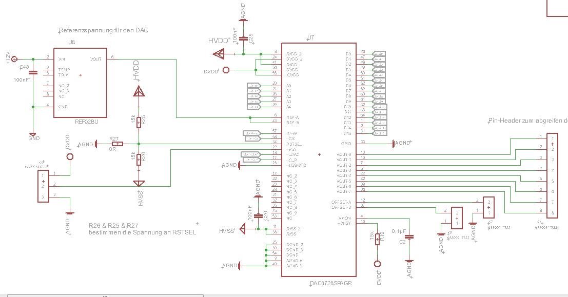
    alright i will atach a scrennshot of the dac schematic...hope thats ok

    some explains to the schematic... HVDD is 15V, HVSS is -15V, DVDD is 3.3V,

    in addition i changed  the voltage devider of the RSTSEL-pin so there apply 3.3V

    what do you mean with the power pad i ?? is it named different in the data sheet? i can't find it?

    thanks stricker

  • and i also got strange values after powe-on reset....
    as shown in table 8 in the data sheet... it must have 0V when: the RSTSEL-pin = IOVDD & ~USB/BTC-pin = GND
    but my DAC gives out 5 V ????
    thx for helping
    stricker
  • Stricker,

    ser str said:
    what do you mean with the power pad i ?? is it named different in the data sheet? i can't find it?

    What I meant by "power-pad" was "thermal-pad". As you can read in page 10 of the datasheet, it is recommended that you connect it to AVSS or leave it floating.

    Thank you for sharing the schematic. It seems like everything is correctly connected.

    1. Are you following the power-on sequence specified on page 41 of the DAC8728 datasheet?
      1. This would be my biggest suspect. The power-on sequence is very important. If it is not used correctly, the internal registers of the device will not power-on correctly and can cause the device to behave abnormally.

    2. Are you using the package with the thermal pad? What voltage do you have the thermal pad connected to?
      1. This can sometimes cause strange behaviors if not connected correctly
    3. Have you verified that the voltage at RSTSEL is 3.3V?
    4. Can you share a scope capture of the SPI interface?

  • Hi Eugenio,
    1. yesterday I've looked into the power on sequence ---> AVDD & AVSS comes first ---> DVDD & IOVDD are the second ---> VREF is the third
    is that a problem???
    2. no i don't have a thermal pad!
    3. yes i'm sure thre are 3.3V
    4. i will try to get a scope capture.....

    ok at the moment I'm at a loss what's the problem and i will order a second dac just to eliminate the posibility of a defektive divice...

    if you got another idea please let me know...

    best regards stricker
  • alright eugenio,

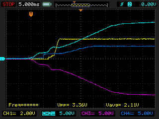
    first i got a scope picture of my start sequence for your , please have a look on it...

    ch1 = DVDD & IOVDD

    ch2 = AVDD

    ch3 = AVSS

    ch4 = VREF

  • The problem might be with the power-on sequence.

    By the looks of your scope capture it seems it follows this order:

    1. AVDD/AVSS
    2. VREF
    3. DVDD & IOVDD

    The datasheet requires:

    1. DVDD & IOVDD
    2. AVDD/AVSS
    3. VREF

    There are registers inside of the device that are not correctly initialized when the power-on sequence is violated.

    The most important part of the power-on sequence is having DVDD & IOVDD power-on first. They are what set the internal DAC registers to their correct states. The rest of the power-on sequence is to minimize the current consumption from the device.

    Can you test the circuit while following the power-on sequence?

  • Hi Eugenio,

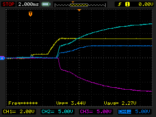
    well i've changed my circuit and my start sequence looks like that now...

    but the strange behavior is still existing !

    ok...then i've put some pull up resistors on the ~CLR & ~LDAC pins
     ----> but nothing changes !

    then i've made a software loop for one output-chanel and gave out every single data-bit....(i've forgot to make that picture with the osci...and will be able to make it next tuesday! ) but i've noticed that when the bits in the middle ( DB5 - DB12) are applying nothing happens...the other are alright.

    I mean i can meassure the 3.3V applying at the DAC-pin directly but  nothing happens at the output!

    have you some another ideas...i'm a little bit frustrated.

    thaks for helping

  • another question ... are the divices checked for right function before delivering ?
    sorry for that question but at the moment i'm in doubt about everything !
    best regards
  • Hi Stricker,

    I understand your frustration. There is nothing worse than debugging a circuit in a lab for hours at a time with no progress!

    Don't worry we will solve this issue.

    ser str said:
    well i've changed my circuit and my start sequence looks like that now...

    The ramp looks much better now. It still worries me that the digital ramp has a long step at ~0.5V. I've seen this cause problems in other devices, so I would suggest attempting power-on using a cleaner ramp.

    ser str said:
    then i've made a software loop for one output-chanel and gave out every single data-bit....(i've forgot to make that picture with the osci...and will be able to make it next tuesday! ) but i've noticed that when the bits in the middle ( DB5 - DB12) are applying nothing happens...the other are alright.

    It would be useful to get a few captures of the digital interface.

    And, answering your question, yes these devices are tested after they are fabricated. To my knowledge the distributors do not test the devices themselves.

  • allright next time i'll be at the firm i wil send you some captures....and i will change the start sequece ....thx for your patience

  • Hi Eugenio,

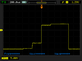
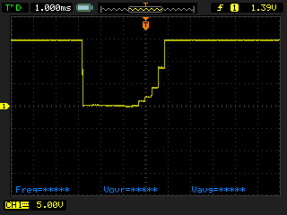
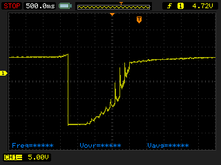
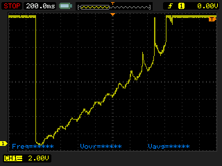
    alright i got the captures a little bit earlier...well please take a look at them

    1. this capture shows every bit from 1-16 with +/-15 V supply and default offset

    2. the 2nd one has the same settings exept an offset of zero...

    the 3rd and the 4th have a loop wich gives out values from 0 - 65535...

    3.  default offset

    4. offset of zero

    perhaps now you have some ideas whats wrong

    thx a lot

  • hi eugenio,

    did you looked into the scope pictures?

    what do you think about them???

    best regards stricker

  • Hi Stricker,
    Thank you for sharing the output plots. I do see the problem that you described.

    Apologies for the late response the message went under my radar. Like I said, I would like to see captures of the digital interface to verify that it correct. Do you think you can share these with me? Just a couple of example writes should be enough.
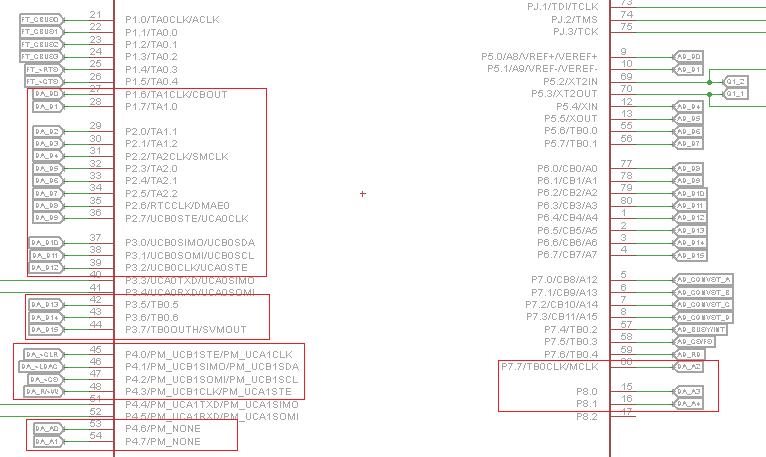
  • yes of course...here we are. this is the msp430F5529 the red boxes are the data & adress bits...don't be scared...i had to connect them like this because the project was began by another guy and

    now i have to shfit the adress & data bits together... : (

    and here some code lines...

    //set dafault dac values

    set_DA_adress(0x0);
        P4OUT &= ~BIT3;                        //R/~W = 0
      
        DA_value(0x8000);                    //
        P4OUT &= ~BIT2;                        //~CS = 0
       
        P4OUT |= BIT2;                        //~CS = 1
        P4OUT |= BIT3;                        //R/~W = 1

    ....

    do {
              
                for(i=0; i<65535; i++){

                        set_DA_adress(DAC_0);                                //DAC adress = 8
                        P4OUT &= ~BIT3;                                        //R/~W = 0
                       
                        DA_value(i);
                      
                        P4OUT &= ~BIT2;                                        //~CS = 0
                       
                        P4OUT |= BIT2;                                        //~CS = 1
                       
                        P4OUT |= BIT3;                                        //R/~W = 1

     P4OUT &= ~BIT1;                                        //toggle ~LDAC ---> gleichzeitige aktualisierung der DAC-ausgänge
                   
     P4OUT |= BIT1;
                   
            }while(1);

    ..........

    and here are the shift operations first DA_value and second adress_value

    void DA_value(unsigned int displValue){                          

      
        // MSB                                                                                                                                           LSB
        //    15    14      13     12      11    10       9       8       7        6        5      4       3        2       1       0
        //P 3.7    3.6    3.5    3.2    3.1    3.0    2.7    2.6    2.5    2.4    2.3    2.2    2.1    2.0    1.7    1.6
      

        unsigned int help = displValue;
        unsigned int copyPort = PAOUT_L;

        help <<= 6;
        help &= 0xC0;
        copyPort &= ~0xC0;
        copyPort |= help;
        PAOUT_L = copyPort;

        help = displValue;
        copyPort = PAOUT_H;

        help >>= 2;
        help &= 0xFF;
        copyPort &= ~0xFF;
        copyPort |= help;
        PAOUT_H = copyPort;

        help = displValue;
        copyPort = PBOUT_L;

        help >>= 10;
        help &= 0x7;
        copyPort &= ~0x7;
        copyPort |= help;
        help = displValue;
        help >>= 8;
        help &= 0xE0;
        copyPort &= ~0xE0;
        copyPort |= help;
        PBOUT_L = copyPort;

    void set_DA_adress (int DA_chanel){          
        // Adress: A4    A3    A2    A1    A0          

        //         P    8.1    8.0    7.7    4.7    4.6
        //            {-------out--------}
        int help = DA_chanel;
        int copyPort = PBOUT_H;

        help <<= 6;
        help &= 0xC0;
        copyPort &= ~0xC0;
        copyPort |= help;
        PBOUT_H = copyPort;

        help = DA_chanel;
        copyPort = PDOUT_L;

        help <<= 5;
        help &= 0x80;
        copyPort &= ~0x80;
        copyPort |= help;
        PDOUT_L = copyPort;

        help = DA_chanel;
        copyPort = PDOUT_H;

        help >>= 3;
        help &= 0x3;
        copyPort &= ~0x30;
        copyPort |= help;
        PDOUT_H = copyPort;

    i've checked the shift-op several time and they seems right....

    thanks for helping

  • Hi Stricker,

    I was hoping to see the output of the digital lines on an oscilloscope. I want to verify that the edges are in the correct places. I know its a parallel interface and there is not much room for error, but it is a possibility.
    I would like to see R/W, CS and a one or two data lines.
  • ohhh sry i understanded that in wrong way...

    i will send you the scopes as soon as possible (think it will be on tuesday)....

  • ok i got it !!!

    THE VREF SHOULD NOT BE GREATER AS DVDD !!!! that was the problem...thx