This thread has been locked.

If you have a related question, please click the "Ask a related question" button in the top right corner. The newly created question will be automatically linked to this question.

DAC8822 strange digital signal in analog output

Other Parts Discussed in Thread: DAC8822

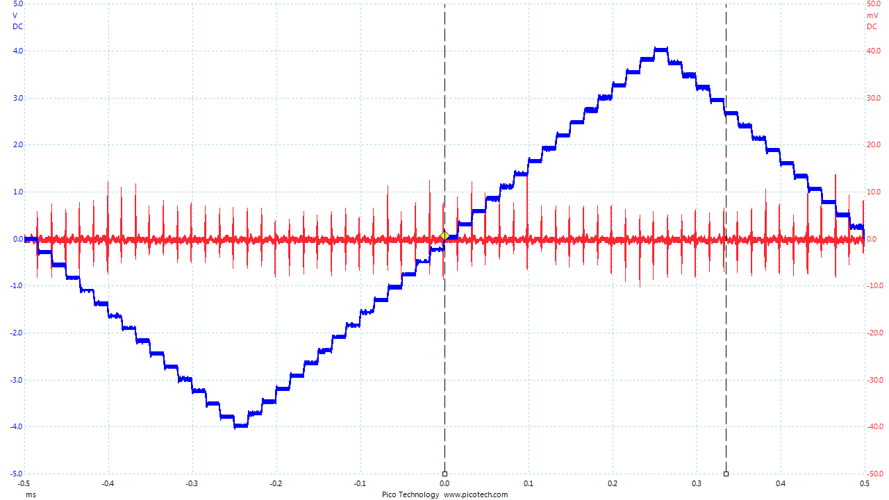
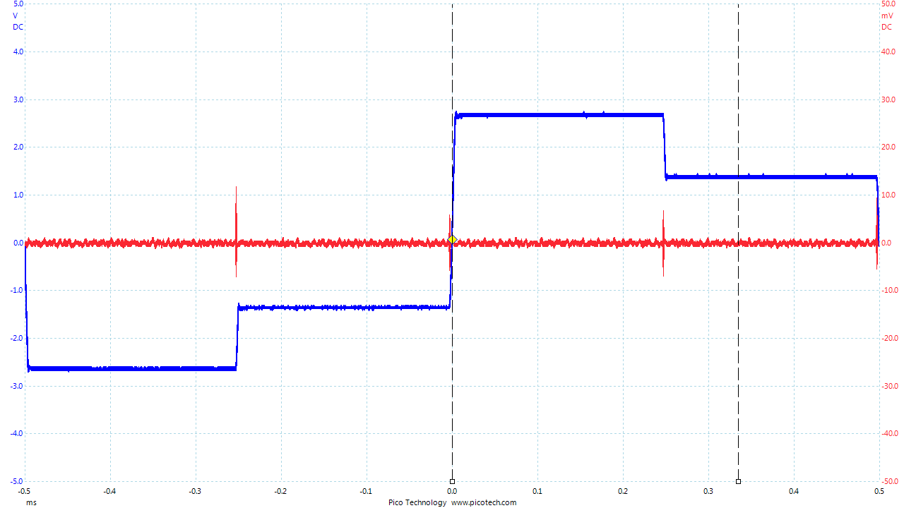
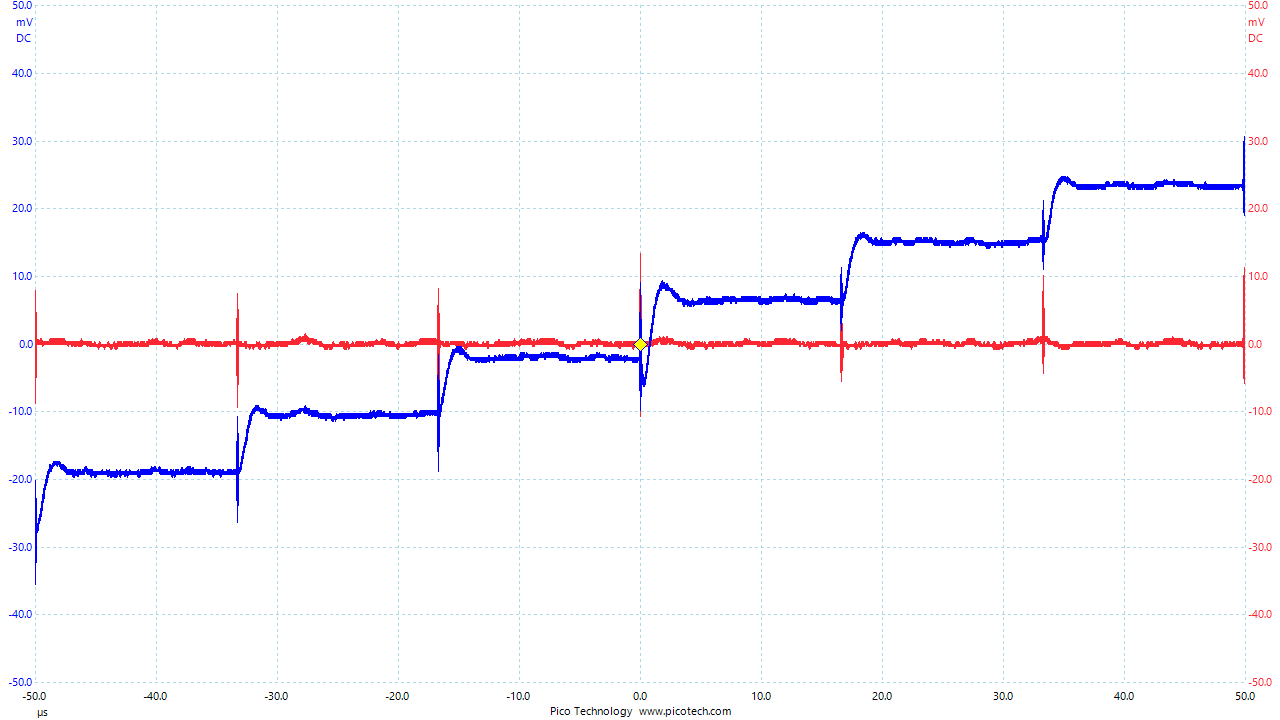
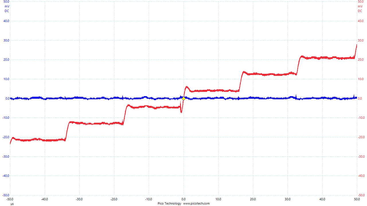
I'm seeing some sort of digital signal embedded in the analog signal of the DAC8822.  In the figures attached, the blue and red are the 2 channels.  The red channel has the same digital code being set while the blue is being changed.  The +/-10mV spikes are happening only when the LDAC signal is toggled, corresponding to the changing analog values on the blue channel.  The 2 figures are at different update rates, showing that the spikes correlate to the update rate.  Are the spikes supposed to be there, or is there a way to get rid of them by proper design?

Any help would be appreciated.

  • John,

    This is most likely digital feed-through, basically the fast-edge transients of the SPI interface are coupling to the output through device-level and/or board level parasitics. The device-level parasitics are specified in the datasheet as 1nV-s but this is conditionally specified with LDAC tied to ground so your use-case isn't exactly 1:1 with the specification.

    A few questions/comments for you...

    •  How are the updates being issued to the DAC in the captures you have provided? Are both DAC A and DAC B data registers being latched with data (one with repeated data and the other with new data) or are you only latching a single DAC data register? Do you require simultaneous updates? The "Input and DAC Register are Transparent" operation described on Page 7 could remove the need for the LDAC pin to toggle complete, which would reduce digital feed-through. The datasheet description is a little ambiguous on this operation and I would want to double-check it in the lab, but weather is keeping me from my lab today and I don't have a convenient test bench ready to go for this part. In the interest of time, could you try this on your board and share your results?
    • Would you mind sharing the PCB and Schematic you are testing this with? As I mentioned, this could be driven by board level parasitics as well, so I would be interested in seeing the design, particularly the layout to see if there are any improvements that could be made there.
    • You could consider adding some series resistance or ferrite beads along with parallel capacitance to the digital lines to slow the fast digital edges to reduce the coupling of the digital signals to the output.

    I hope this helps. If you are unable to test item 1, I will work towards a test setup but it may take some time.

  • Thanks for your reply.

    Update method: Both a & b registers are written to every cycle of the update rate.  Yes, 1 is repeated data and one is new data.

    Simultaneous updates are preferred, but non-simultaneous might be tolerable at fast update rates.

    Transparency: Do you mean that LDAC should be tied high all the time, or that it should still be toggled, but should be high before _WR goes low and then low after _WR goes high?  Is the goal to stretch out the LDAC pulse by a few cycles of the system clock?  My system clock is 100MHz, and I think LDAC would be 4 times longer, meaning it goes from 10ns to 40ns.  Is this what you want to try?  When I slow the update rate in my attached figures, I am running everything at 100MHz, but I just do it less often.  (I just mention it, because I'm not sure what's important.)  Do you want to slow the clock down, as well?  Once I understand what to do, I should be able to rewrite the firmware to try it.

    Can I email you the layout and schematic?

  • John,

    My suggestion was tying LDAC high and removing the step of toggling this altogether, WR would be the only signal moving. Most of our products offer an update method like this, though the DAC8822 datasheet is dated and ambiguous I believe this should work.

    The clock rate itself is only important as far as determining how much we can slow the edges is concerned. Really all we want to do is remove sharp edges on the digital I/O. Regardless of the specific clock frequency I suspect your edges will be just as sharp. If your controller allows to you program the source capabilities for the I/O pads drive strength you might try reducing that to achieve similar effects to adding the ferrite/resistor and capacitor.

    I'm having trouble fetching user data from the E2E right now, so I'll be sending you a message to exchange emails.
  • I changed the firmware to hold LDAC high.  The result was:

    As suggested, I then changed the I/O pad drive strength.  I am using a Xilinx FPGA.  Default seems to be DRIVE = 12mA.  I changed to DRIVE = 2mA.  I get the following:

    I thought this looked nice, so the next thing I tried was to keep DRIVE = 2mA and toggle LDAC again, instead of keeping it high.  I get this:


    This also looks prettier than before.

    Can you please help me make conclusions based on these results?  Is reducing the DRIVE current a permanent solution, or is it a temporary solution that tells us what I need to change on my board revision?  If I need to make a change, what might that be?


    Thanks for all your help.

  • John,

    I appreciate you posting the results from our email discussion to the forum - it's great for results to be shared on the forum for community members who may have similar problems in the future.

    In my opinion reducing the drive current from your MCU is a viable permanent solution.

    A resistor in series can provide the same effect of limiting the current flow between the MCU and the DAC. In the end what we’re really after is removing the sharp edges of the digital signals. A R/C low-pass combination would do the trick. An alternative might be a series ferrite bead – I’m not sure how the cost / performance / size balance plays out, not something I’ve dug into before.