This thread has been locked.

If you have a related question, please click the "Ask a related question" button in the top right corner. The newly created question will be automatically linked to this question.

Design output of DAC8760 for higher currents

Other Parts Discussed in Thread: DAC8760, OPA564-Q1, OPA541, OPA544, OPA177

Dear forum-members,

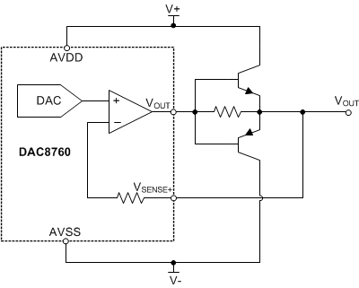
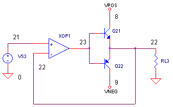
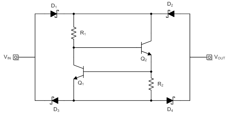
i could use some help and tips concerning some part recommondations to buffer the voltage output of the DAC8760, the DAC itself can only sink and source upto a maximum of 20 mA, but i would want to boost this up, to about 500 mA. How do i go about this, preferably without loosing the 16- bit precision of the DAC.

Any help would be greatly appreciated.

Yours sincerely,

Alex

  • Alexander,

    The most straight-forward way to achieve this high current voltage output is to use one of our amplifiers with high source/sink current capability, these parts used to be in a category called "Power Amplifiers" on ti.com but it looks like that category has been removed. Instead, you can go to the op amp parametric search table and sort by output current.

    There's about 8 options on that page that can source/sink >500mA and that are wide supply to support the full +/-10V span of the DAC8760.

    • OPA564-Q1 is an automotive qualified device and the only one of these 8 parts that supports the -40C to 125C operating temperature span to match up with the DAC8760 operating temperature rating
    • OPA541 has the best input offset voltage drift. If you're performing one-time room temperature calibration on your system and you can live with -25C to 85C operation this is probably your best candidate.
    • OPA544 is the best combination of initial input offset voltage and offset voltage drift, so if you are not performing any calibration this probably your best choice. Slightly wider operating temperature than previous, -40C to 85C.

    Input offset voltage on these high current parts is pretty bad compared to the DAC8760 and typical precision op amps, so if calibration isn't an option these parts may not be acceptable.

    If this approach isn't acceptable, we can explore an alternative where we basically add an external BJT output stage to the DAC8760 output. If you're interested in this approach I can sketch something up.

  • Kevin,

    Thanks for the quick response. I was also considering the addition of a push-pull output stage, as you suggested. But are these more reliable than opamp-solutions? And yes, i woukd greatly appreciate it if you could give a short explanatory sketch of your proposed solution with bipolar transistors.

    Kind regards,
    Alexander
  • Alexander,

    From a purely functional perspective I don't think either approach is more reliable than the other. The buffer amplifier approach is certainly simpler, and therefore may be considered more reliable since it's just another product that you buy and place into your system - responsibility of it's performance being traced back to the manufacturer. The biggest draw-back to these power amplifiers, in my opinion, is the input offset voltage and the input offset voltage drift. Depending on the output span you're using, those error sources may or may not be considered significant so these parts may be usable.

    Adding the output stage is certainly more complex and will require careful selection of the additional transistors and potentially some extra work to stabilize the output depending on what the output is driving. I haven't actually built this myself yet so I can't speak to a size/cost comparison back to the power amplifier approach.

    This is what I had in mind:

    The external resistor placed in this design can be considered optional, the idea is that this will help reduce the cross-over distortion between when the PMOS and NMOS are active. In normal operation the DAC8760 output amplifier sources most of the current to the load, until the current pulled by the load causes the DAC8760 output amplifier output voltage to rise ultimately raising the Vbe of the two output transistors and allowing them to source the output current. The feedback node is taken from the other side of the bipolar transistors. Without the resistor the output amplifier just controls the Vbe voltages and allows the bipolar transistors to source the entirety of the current to the load while the output amplifier just watches the voltage across the load for feedback.

  • Kevin,

    i also think a simple push-pull solution should do the trick. I also came across this solution. In this article, several push-pull solutions for low distortion are highlighted. The last example seems very interesting to me. I tested this with an OPA177 amplifier and a PNP and NPN darlington pair. This seemed to work very well. The only question i was asking myself, is where exactly in this design should i connect the VSENSE+ of the DAC8760. And what would be the best solution for overvoltage-protection of the output. Overcurrent protection can be achieved through a simple pair of transistors that will redirect the base current of the darlington transistors as soon as a sufficient current is passing through a pair of sense resistors. But i don't really know where i should place the overvoltage-protection.


    If you could give me some suggestions concerning this topic, i would be very grateful.

  • Alexander,

    You're referring to this circuit from the link you posted, correct?

    This circuit is basically the same as the one that I have suggested, except that they do not include the series resistor directly connecting the buffer output to the load. You would connect the VSENSE+ pin in the same way that I showed in the diagram I posted previously. VSENSE+ is the feedback path, so it goes to the feedback network and to the inverting input pin. I think this should answer the first part of your question?

    Concerning your over-current and over-voltage protection schemes, are you trying to protect the system from external sources damaging your output stage or are you designing a circuit to ensure that your output stage does not perform out of spec? I don't have a diagram ready but I think I follow what you're suggesting for the current limiter. For the voltage stage I think I would just use a simple TVS diode or clamp-to-rail diode. I'm not sure exactly what you want to be doing with the circuit, please elaborate and we can see what we can come up with.

  • Kevin,

    The actual purpose of the circuit is a programmable voltage source that could be used to apply voltage over all kinds of different loads. Thats why i want to protect the output from overvoltage from external sources.

  • Taking a look at previous circuit. If i use darlington transistors with a nominal current gain hFE of 4000 then would this be sufficient enough to make sure that the base-current supplied to the transistors and althus sources by the dac wouldn't exceed the 20mA limit? Absolute maximum current that i would sink or source is about 500mA, so divided by approx. 4000, this wouldn't translate itself in an significant base current drive so no problem for the DAC to provide this current. Correct me of i'm wrong.
  • Alex,

    You'll have to forgive my delayed response, I was meaning to get to this but lost track of time yesterday.

    Here's a current limiter I've built/tested previously with good success:

    Basically the default or primary path of current flow is always through Q2 and R2. Diodes D1, D2, D3, and D4 rectify this current path no matter what the polarity of the current flow is. When excessive current is flowing through Q2 and R2, the voltage drop across R2 raises which turns on Q1 and sort of "suffocates" Q2 creating our current limiter. Sizing R2 is all about where you want to place the current limit, sizing R1 is less scientific - it just needs to be small enough to ensure that during normal operation Q2 gets enough base current but still large enough to maintain the effectiveness of the current limit because as Q1 turns on we don't want to provide an alternative current path - we just want to choke Q2. I would suggest you just set the R2 value first then in SPICE muck with R1 until you get the behavior you want.