This thread has been locked.

If you have a related question, please click the "Ask a related question" button in the top right corner. The newly created question will be automatically linked to this question.

Making own ADS8556 Card?

Other Parts Discussed in Thread: DAC8728, ADS8556, DAC8728EVM

Hi
I have a system that contains, 2 ADS8556EVM, 1 DAC8728EVM and 1 Altera FPGA boards and sensors etc. 2 ADC card take analog voltage and current signals from sensors and after converting to the digital send to the FPGA. FPGA makes some calculations and sends the digital data to the DAC for converting to analog again.Because of an electricity fault all the chips on the (ADS and DAC) boards had burned. I had ordered free chips (ADS8556 and DAC8728) from TI as sample. I changed old burned chips with the new ones. DAC8728EVM perfectly worked but ADS8556EVMs did not. I coul not find the cause of problem. During the electricity fault probably some other things had also burned. So I decided to make my own card that contains all chips (ADC and DAC) together. So i need some help because of high frequency characteristics of the ADS8556 chips. Can anyone please answer my questions?
1- FPGA card has 2 40 pin expansion header for I/O. 4 pins of these headers are dedicated for GND out. There is not another possibility to connect FPGA's GND and ADC-DAC Card's GND. Can the cable connection in the fig. 1 provide a clean ground connection? Or shall I mount the ADC-DAC card directly on the FPGA male expansion header pins with female ones?


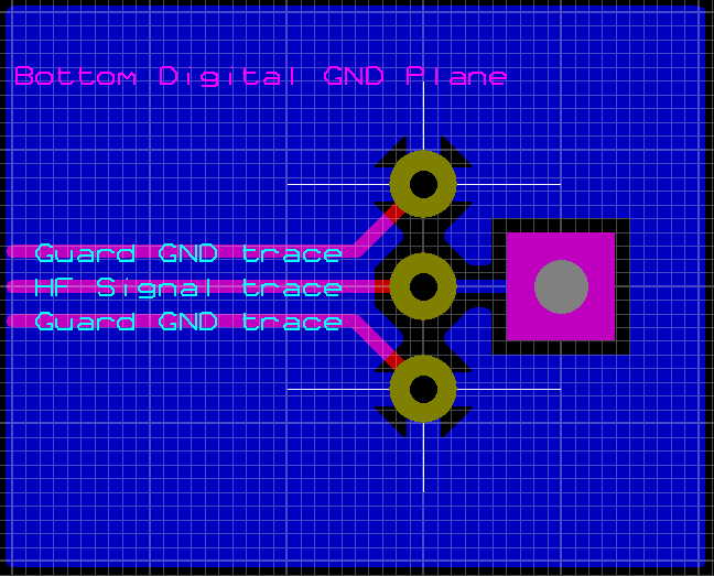
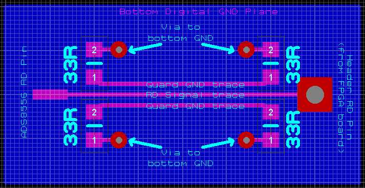
2- I had encountered some noise problems with the current (burned) system. After time-consuming investigations and long trial-and-error processes I had reached a solution by using a shielded cables for "RD" and "HOLD" signals. But apperance was very bad. This time i don't want to use any cable. Can the layout in figure 2 help me about this issue?
Thanks for your answers...

  • Hi Huseyin,

    Welcome to the e2e forum!  For the board interconnect, there are 'extended' female sockets available from Samtec where the pins go through the board and might provide enough length that you could either mount both your FPGA and ADS8556 directly by plugging them together.  You could also use your IDC ribbon cable approach.  If there is a ground plane on both boards, the four connections should be sufficient.

    Using a ground ring around sensitive signals is acceptable, but you might also consider terminating the lines with a small (~33 0hm) series resistor.

  • Thanks for your answer.

    - FPGA board is a proffesional board and probably it has multilayer pcb configuration having a ground plane. But the ADC-DAC board that i will design has a two layer configuration and bottom layer is ground plane except some jumping traces.(I don't know the exact word. I mean a trace goes bottom layer by via then moves at the bottom layer and again to the top layer by via). Is it still OK?

    -33 ohm series resistor to the ground traces (as in the fig.)?

    Note: If I want to ask some other questions about this issue can i go on with this post or open new one?

  • Hi Huseyin,

    I meant for you to put the R in series with the actual RD(?) signal, you don't need it on the guard ring.  Yes, you can continue to use this thread if you have additional questions about the ADS8556.