Hello
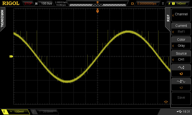
I have a problem with glitches in my signal generator for diploma thesis based on DAC5672. I know that glitches aren't something abnormal in DACs, but i would like to find out information about normal levels that can be achieved by DAC5672, because I cannot find any info in datasheet. I've attached picture from scope.
The major carry glitch on signal 1kHz, 400mV p-p is 200mV with duration(width) of 6ns measured with probe with short ground lead on current output of DAC with current to voltage conversion on 25Ohm resistor without any filtering.
CLKIQ and WRTA are connected.
The reason why I ask is because I cannot find some suitable solution or I don't know if I'm spending time on finding solution which doesn't exist.
Sample rate that I can reach with FPGA is 230 Msps which can be used to generate approximatelly 70MHz sine wave. The main thing is that if I use low-pass filtering, I have to design filter (or put a cap between current outputs)
with corner frequency of few MHz, maybe 10MHz, to sufficently filter those glitches. Then the bandwidth of my generator will be so small that the FPGA and the speed of this DAC doesn't have any sense.
The sample and hold solution is way too complex to ensure good timing. I've spend many many days trying to reduce those glitches by different ways, but I'm lost.
Are those levels normal? Can they be reduced without sacrificing almost all of the bandwidth? Or can they be caused by a some mistake in layout?
Thank you
Miroslav Šíma