This thread has been locked.

If you have a related question, please click the "Ask a related question" button in the top right corner. The newly created question will be automatically linked to this question.

problem using ads1247

Other Parts Discussed in Thread: ADS1247, DAC7568

We are experiencing some problems using a ads1247. It's not giving us reliable results.

We spend quite some time with code snippets from the TI forums, but no result yet.

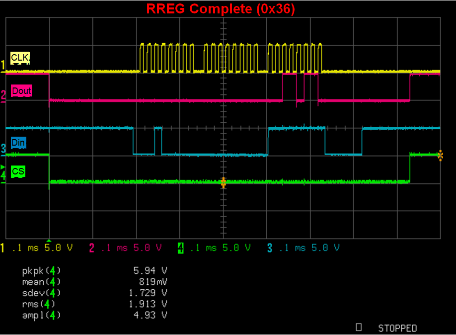
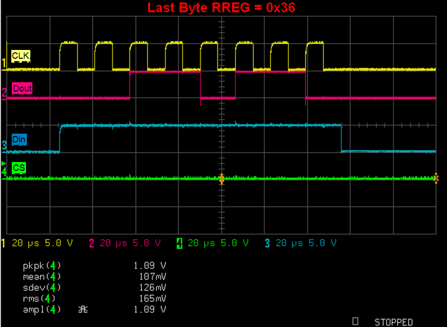
Debugging the issue, we first tried to read the internal temperature diode. But doing that showed that even reading back the registers with the RREG command does not work reliable. And furthermore the RDATA results do not make sense.

Sometimes we read back the correct result, but most of the times not.

We use the following code to drive the chip.

def ads1247_smalltest(spi):
    """Basic test sequence to test ads1247
    """

    CS = PIN_LOCKIN_CS3
    RDY = PIN_DAT_RDY3
    START = PIN_START3

    spi.mode = 0b01

    GPIO.output(START, True)

    GPIO.output(PIN_RESET, False)
    time.sleep(0.001)  # >4 cycles
    GPIO.output(PIN_RESET, True)
    time.sleep(0.002) # >0.6ms

    GPIO.output(CS, False)

    spi.xfer2([0x6])  # RESET
    time.sleep(0.002) # 0.6ms

    spi.xfer2([0x16])  # SDATAC

    GPIO.wait_for_edge(RDY, GPIO.FALLING)
    spi.xfer2([0xff, 0xff, 0xff]) # dummy read

    # MUX0, VBAS, MUX1, SYS0
    spi.xfer2([0x40, 0, 0x1])
    spi.xfer2([0x41, 0, 0x0])
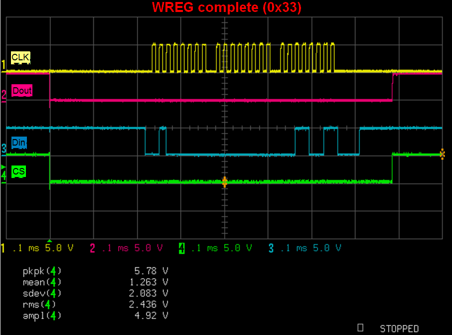
    spi.xfer2([0x42, 0, 0x33]) # internal temp 
    spi.xfer2([0x43, 0, 0x4F])

    time.sleep(1)
    # read back the registers  (they do not read back correctly !)
    data = spi.xfer2([0x22, 0, 0xff])
    print "MUX1 %x" % data[2]
    data = spi.xfer2([0x22, 0, 0xff])
    print "MUX1 %x" % data[2]
    data = spi.xfer2([0x20, 0, 0xff])
    print "MUX0 %x" % data[2]
    data = spi.xfer2([0x20, 0, 0xff])
    print "MUX0 %x" % data[2]

    # IDAC0, IDAC1
    spi.xfer2([0x4a, 0, 0x06])
    spi.xfer2([0x4b, 0, 0x1])


    while True:
        GPIO.wait_for_edge(RDY, GPIO.FALLING)

        data = spi.xfer2([0x12, 0xff, 0xff, 0xff])
        result = data[1] << 16 | data[2] << 8 | data[3]
        print "result %x" % result

    GPIO.output(CS, True)

The output is 

MUX1 c0
MUX1 81
MUX0 4
MUX0 0
result ff8020
result 408102

You see, i read back mux1 with different values, (both not the ones we actually set). 

Our digital connection (SPI) seems somewhat ok though, we are able to blink a led via GPIO0 (REFP0). 

Anyone having a suggestion how to drive the chip, to measure its internal Temp ?

What we want to accomplish (after we've seen that reading the temp works) is measuring two voltages alternating. (AIN0, AIN1: both compared to AIN3 (connected to GND).  Any tips on how to drive this ? 

Thanks,

Harm

  • Harm,


    Earlier in the month I wrote a blog about debugging digital communications. Read through it first to see what could apply to your communication problem. You can find a link to it below:

    e2e.ti.com/.../help-i-can-t-talk-to-my-data-converter-what-s-wrong

    After that, I'd try to get an oscilloscope plot to make sure that you're communications match the timing diagrams in the datasheet. Better yet, I'd get a logic analyzer readout of the communications.

    Looking back at the post, my first guess is that your problem is the version of SPI that you're using. The output data is set up by the rising edge of SCLK and clocked out at the falling edge of the SCLK. Also, SCLK should dwell low. Make sure that the /CS line is low for the entire transaction, and not just byte-to-byte.

    Another possibility is that the output is being interrupted by a new data conversion. If a /DRDY indication is given, it will immediately update the DOUT register.

    Regardless, get an oscilloscope reading with SCLK, DIN, DOUT, and /DRDY. If you have a have a logic analyzer, look at /CS too.


    Joseph Wu
  • >Looking back at the post, my first guess is that your problem is the version of SPI that you're using

    Yeah, that was the first thing we though too. But we're using the right one. CPOL=0, CPHA=1. (tried all 4, this was indeed the best). Driving an other TI device on the same board works just fine (DAC7568).

    We've inspected the SCLK, DIN, DOUT, CS on a good scope. all signals looked clean& valid. The DOUT returned with RREG command, looked clean. DOUT perfectly stable at falling clocks.  CS is driven ok.

    We could perfectly manually decode  the SPI data in and out, by looking at the scope image.

    When writing registers we do not read back the correct values.

    when writing 0-8 to MUX0, we read back the correct value. when we go higher, the lowest 3 bits of the register value gets shifted left one. (same with MUX1, and others)

    WREG RREG
    0x1 0x1
    0x3 0x3
    0x9 0xa
    0x13 0x16
    0x30 0x30
    0x33 0x36
    0x38 0x38
    0x39 0x3a

    Confused why this happens. Looking at the scope, those shifted bits in RREG, actually look perfectly clean (but wrong) on DOUT.

    When compensating for this shifting.... (carefully choose what to write to the registers). we _are_ able to read the internal temperature. (~ 0.117 V)  

    But thats not a solution, we cannot set the MUX[01] to the values we actually need in our application. (eg: we need 0x13 in MUX0).

    We'll check if we can do tests on an ads1247 development board.

    Regards,

    Harm

  • Harm,

    Why don't you post a scope shot of a bad read/write transaction for the device. It couldn't hurt to have a look at what could be wrong.

    Joseph Wu

  • Harm,


    Also, what bandwidth is the oscilloscope that you're using? If you have noise on SCLK, the scope needs to be fast enough to pick it up.

    The thing that concerns me is that I can see some inconsistencies in how the error appears. In the last four readouts:
    0x30 0x30 - no error (but no 1s in the second nibble)
    0x33 0x36 - bit shift error
    0x38 0x38 - no error (with 1s in the second nibble)
    0x39 0x3a - added bit (or bit shift + added bit)

    None of these look exactly the same. Are all of these readings consistent? Do you get the same error each time?

    You might want to see if loading down the SCLK with some small amount of capacitance helps so that it cleans up the SCLK, just in case some small amount of noise is coupling in. You'd have to play with different values and look on the scope to see how the loading affects the SCLK waveform.

    Regardless, I'd still like to see the original scope photos of the write and the readback.


    Joseph Wu
  • Well they are all the same (kinda)

    There is a bit shift error in the last 3 bits, not the last nibble.

    0x30 0x30 - no error ( no 1s in the last 3 bits)
    0x33 0x36 - bit shift error     011   -> 110
    0x38 0x38 - no error (no 1s in the last 3 bits)
    0x39 0x3a - bit shift error in last 3 bits.  ( 001 -> 010)    whole nibble is: 1001  -> 1010

    The readings are very consistent. I read the same values every time.

    >Also, what bandwidth is the oscilloscope that you're using? If you have noise on SCLK, the scope needs to be fast enough to pick it up

    Hm.. right. I'll check this. 

    Still weird though..  clock noise should give me inconsistent readings. random bits would flip.

    (I did the tests with a relative slow SPI clock (100KHz))

    I'll have more results on Tuesday. (I'll have a development board too then). I'll reproduce the scope images too then. (and attach)

  • Find attached some scope images of SCLK, DIN, DOUT, CS that demonstrate the problem we are seeing.

    The sequence executed is an infinite loop of the following two commands:

    while True:
       WREG: 0x40, 0x00,0x33     // write MUX0,  one byte, value 0x33
       RREG: 0x20, 0x00,0xFF     // read MUX0,  one byte
    
    with 0.5s sleeps between any commands
    

    The RREG always reads back 0x36  instead of 0x33.  This is 100% consistent.

    SPI clock is 100Khz, measurements done on a 500MHz scope.

    A detailed snapshot of the last byte shows the 0x33 written (0011 0011)

    RREG

    For read

    ing we send 0x20, 0x00, 0xFF.  We read back 0x36 (instead of the expected 0x33)

    A close-up of the last RREG byte shows the 0x36 (0011 0110) on DOUT. easy to manually decode on the falling clock edges.

  • Harm,


    The waveforms look clean and I agree that the device is reporting back something other than what you wrote into it. I assume that you have issued a SDATAC to prevent the data from interrupting the DOUT register when you are reading it out?

    Just looking at the communications, there are two things that I would try to change in the write setup. First, I'd try to have DIN low when the /CS goes low. Second I'd try to keep the DIN from changing between the last SCLK and the rise of /CS. I can't say that either would cause this problem, but at this point it's something to try.

    I may have some more recommendations in the morning, but I'll have to check on something in the design.


    Joseph Wu
  • > I assume that you have issued a SDATAC to prevent the data from interrupting the DOUT register when you are reading it out?

    Yes.

    > First, I'd try to have DIN low when the /CS goes low. Second I'd try to keep the DIN from changing between the last SCLK and the rise of /CS. I can't say that either would cause this problem, but at this point it's something to try.


    I'll check if I can do that. (I drive the pins via a raspberry pi board, so I have to figure how how to control DIN directly. thats typically handled automatically). (only CS is driven directly by me).

  • Harm,


    Here's an additional question that we thought up here. How long do you wait after power up before you start communications with the device? Once the device has powered up, there is a 16ms time period where you cannot communicate with the device (assuming a 4MHz clock). You can see this in the SPI communication example on page 55 in Figure 83. If you have not waited this time, the SDATAC and the RESETs may not have been received by the device.

    I would start by adding a 16ms delay after the START pin rises. This would give enough time to ensure the device has come up properly. After that, I'm not sure you need the RESET command or the RESET pin toggle. The device should have come up correctly into its default state.


    Joseph Wu
  • sprinkling around 100ms sleeps is not helping. -> no change.

    We did find however that with a development board (ads1247 EVM) all works as expected. Still puzzled why.....

  • We found something more.

    We have 3 boards connected with our main board. all three with an ads1237.

    We see that if we
    * connect only one board all works.
    * connect two boards (but only use/test one), it works often, but not always. (we read back correct register values 80% of the time).
    * connect three boards (but only use/test one), it never works. the registers read back incorrect data.


    This seems to indicate to SPI problems. ( the ads1247 EVM seems more resilient)
    So although initially the SPI lines looked clean on the scope, as posted in this thread, we're going to change the main board to improve these (especially the SCLK).

    its not a CS problem, as we're able to blink a led via ads1247 GPIO on each board individually.

  • Yes the problem was caused by our SCLK. it was not clean enough. The rising edge of SCLK was not steep enough. (and wobbled a bit, causing the ads1237 to see a falling edge too).

    Lowering the resistors of the level translators for SCLK fixed it for us.