


Other Parts Discussed in Thread: ADS8556, DAC8728, DAC8728EVM
Hi Tom,
I wanted to continue with the other thread (Making own ADS8556 card?) but I could not see any "Reply" button. So I decided to open new one. After a long while I am continuing to design my adc-dac card. I have new questions;
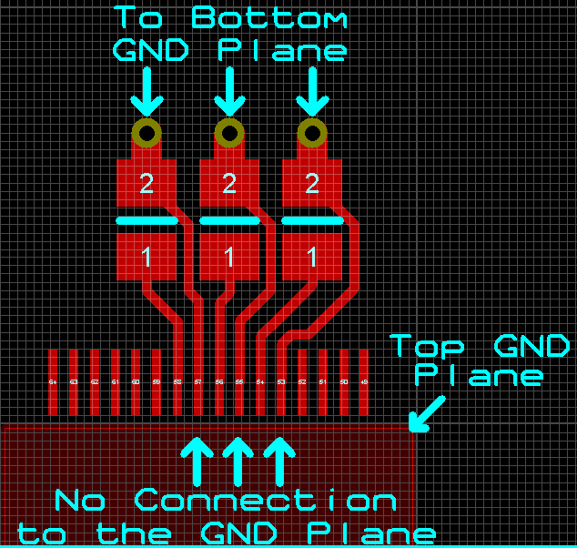
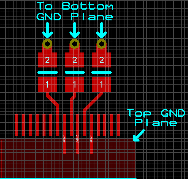
1- In ADS8556 manual at page 13 there are expressions for the REFC_A (pin 54), REFC_B (pin 56), REFC_C (pin 58) and REFIO (pin 51). "Connect a 10 uF ceramic decoupling capacitor between this pin and pin 53 (or 52,55,57)". Also there is an article written by Matthias Taenzer (Texas Instruments' Nyquist ADC group) at below link which also supports same layout. But when I looked at the ADS8556EVM gerber files, I realized that Pins 52,53,55 and 57 are connected directly to the top GND plane, not to the capacitor leg. So I am confused. Which layout gives best result?
Layout2
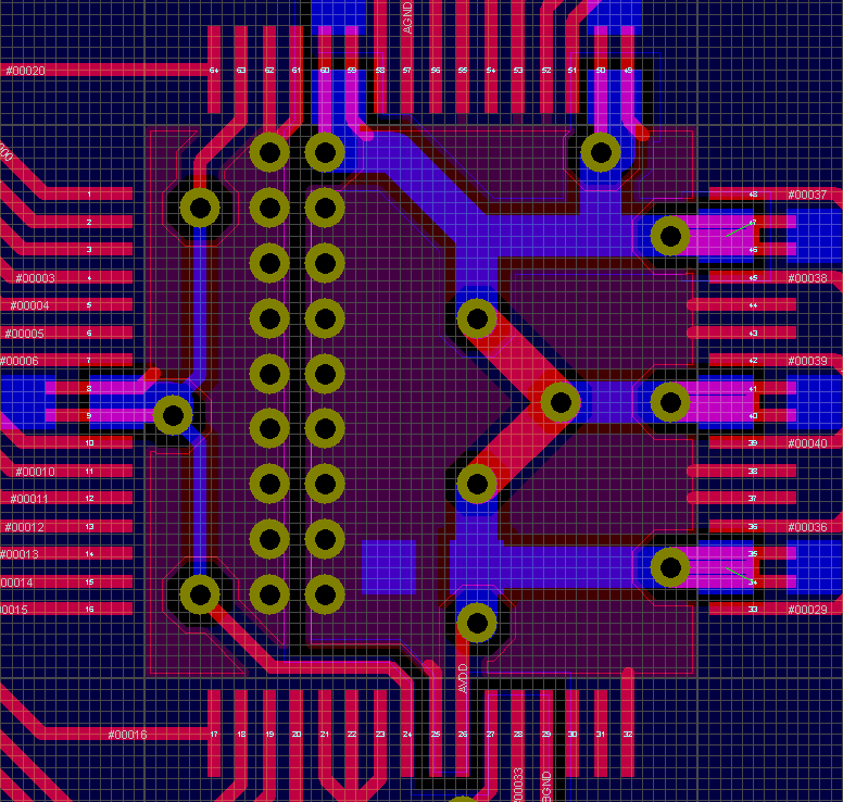
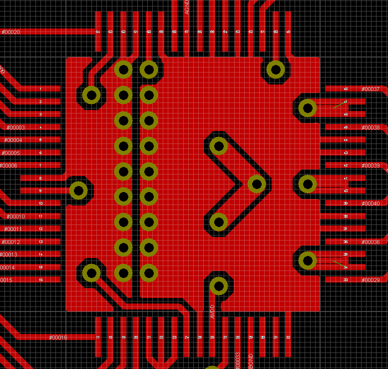
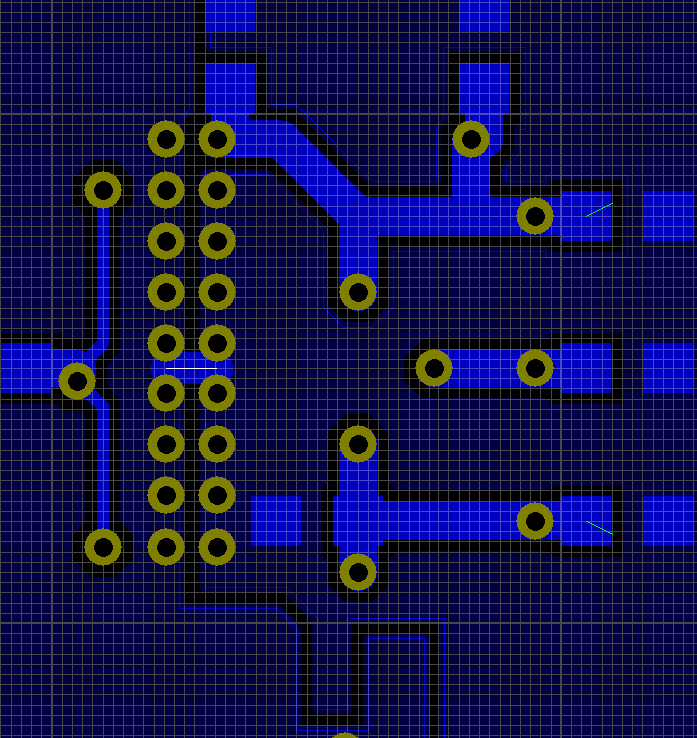
2- Could you please glance my layout for one ADS8556 chip? (There will be one more ADS8556 and DAC8728). I used 2 layer board. Bottom layer is almost dedicated for AGND and DGND. Only the area under the chip is a little splitted due to the lack of AVDD layer. I placed 100 nF decoupling capacitor just under the chip. I used one capacitor for adjacent AVDD pins (34-35, 40-41, 46-47) as ADS8556EVM. AGND and DGND are connected only at one point at the bottom layer. Does this layout give me acceptable results?
Bottom and top copper together
Only Top copper
Only bottom copper
Thanks alot for your answers
Best regards

