This thread has been locked.

If you have a related question, please click the "Ask a related question" button in the top right corner. The newly created question will be automatically linked to this question.

Porting ADS1015 driver to ADS1014

Other Parts Discussed in Thread: ADS1014, ADS1015

Hi,

We are using ADS1014 in our design in single differential mode. Two FSR output from an Op AMP is connected to AIN0 & AIN1 of ADS1014.

We have taken reference of ADS1015 driver from TI SDK 7.01 (Linux kernel 3.12) and ported to ADS1014. Following are the changes done in the driver.

//config |= (channel & 0x0007) << 12; commented Multiplexing configuration, since ADS1014 doesnt support Multiplexing

static const struct sensor_device_attribute ads1014_in[] = { SENSOR_ATTR(in0_input, S_IRUGO, show_in, NULL, 0), /*GH: As only one differential signal is connected to ADS1014, we limit the channel numbers to 1 */ // SENSOR_ATTR(in1_input, S_IRUGO, show_in, NULL, 1), // SENSOR_ATTR(in2_input, S_IRUGO, show_in, NULL, 2), // SENSOR_ATTR(in3_input, S_IRUGO, show_in, NULL, 3), // SENSOR_ATTR(in4_input, S_IRUGO, show_in, NULL, 4), // SENSOR_ATTR(in5_input, S_IRUGO, show_in, NULL, 5), // SENSOR_ATTR(in6_input, S_IRUGO, show_in, NULL, 6), // SENSOR_ATTR(in7_input, S_IRUGO, show_in, NULL, 7), };

Also, commented in1_input to in7_input, since we are using single differential input on ADS1014.

#define ADS1014_CHANNELS 1 -> Changed channels from 8 to 1.

Please let us know, if  these changes are ok or something else needs to be changed for supporting ADS1014.

While testing, when force is not applied on FSR (RV1 & RV2) 0V is applied to AIN0 & AIN1 and ADC reading is 0.

When force is applied only on RV2, 2.5V is applied on AIN0 and 0V on AIN1 and ADC reading is measured as 2048.
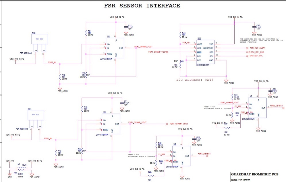
However, when force is applied only on RV1 2.5V is applied on AIN1 and 0V on AIN0 and the ADC reading is measured as 129087. This reading seems to be wrong. Also, when both the FSR are pressed, ADC reading is measured as 129087. Ideally, when both the FSR are pressed, approximately same input voltage is applied to AIN0 & AIN1. However, ADC reading is measured as 129087. Please let me know, if I am missing something here. PGA is set to 2 and data rate as 4.

Please let me know, if the changes done to ADS1015.c for supporting ADS1014 is valid.

Attached the snapshot of FSR & ADS section herewith.

Request your help on this.

  • Siva,


    The ADS1014 is going to be a subset of the ADS1015 and the code to use the device should be similar. Even in the bits that control the multiplexer in configuration register won't affect the ADS1014 since those bits are disabled. So even if you used the same code, the ADS1014 wouldn't respond to the ADS1015 mux configuration changes. It would ignore the changes and continue to use it's only inputs. In that respect, I don't know if you need to change anything at all.

    Since the ADS1014 is a 12-bit ADC, the largest full scale reading that you would be able to get out of the device would be 2047 (0FFFh). You mention that you're getting a reading of 129087, which only makes sense as a negative number of 18 bits in representation. Instead, I would try to measure the ADC input with a multimeter to compare the input with the actual output code coming from the ADC. This is better to make sure ADC is working correctly.

    When it comes to the code, I don't think that we're going to be of much help. This code did not originate from the product group to which the ADS1014 belongs, so I don't know much about where it came from and how to use it. You mention that this code originated from the TI SDK 7.01 (Linux kernel 3.12). Is this from the Sitara Processors Group? If so, the Sitara forum may be of some help.


    Joseph Wu
  • Hi Joesph,

    Thank you for your quick reply.

    Yes, I measured the input voltage on the ADC input.

    1) When input to AIN0 is 2.5V and input to AIN1 is 0V, output code was 2048.

    2) When Input to AIN0 is 0V and input to AIN1 is 2.5V, output code was 129087. This I believe is negative input, but the output code looks out of range.

    3) Also, when input to AIN0 is ~2.5V and input to AIN1 is ~2.5V, output code is also 129087 instead of close to 0.

    Please let me know, if something is wrong, since getting out of range value for 2) & 3)

    Regards,
    Siva
  • Siva,


    The ADS1015 is a 12-bit converter. The maximum output when the input is positive full scale is 2047d. From the output data will be 0FFFh since the first four bits are padded with zeros.

    When the input is at negative full scale, the output should be 63488d or F800h. In this case the output is much larger than 129087. The ADC is not putting out enough bits to give you that number. It looks like what ever output you are reading is about 2x the correct value, or your firmware is bit shifting in an extra digit.

    I would start by making sure that the ADC is putting out a similar number to F8000h. Get an oscilloscope or logic analyzer and make sure that the ADC is putting out the correct digital output. Then compare this output to whatever your firmware gives you. Since I don't really know the firmware, I'm not really able to help you much with debugging.


    Joseph Wu