


Hi all,
I'm working on a hobby project and am trying to interface the ADS1248 to a Raspberry Pi to measure liquid temperatures (0-100 deg C) with a 100ohm RTD. I seem to be communicating with the chip just fine (can set and read the registers), however every time I attempt a conversion I get the same result (exactly mid-range) from the ADC. This is hardly my area of expertise (I mentioned this is a hobby project), and I'm hoping there's an obvious mistake that I can't find that someone here can point me to. I've read the data sheet and am basing the design off of the 'Hardware-Compensated Three-Wire RTD Measurement' design example. I've double-checked the wiring and the schematic and I'll admit I'm stumped -- I just can't get any data from the ADC.
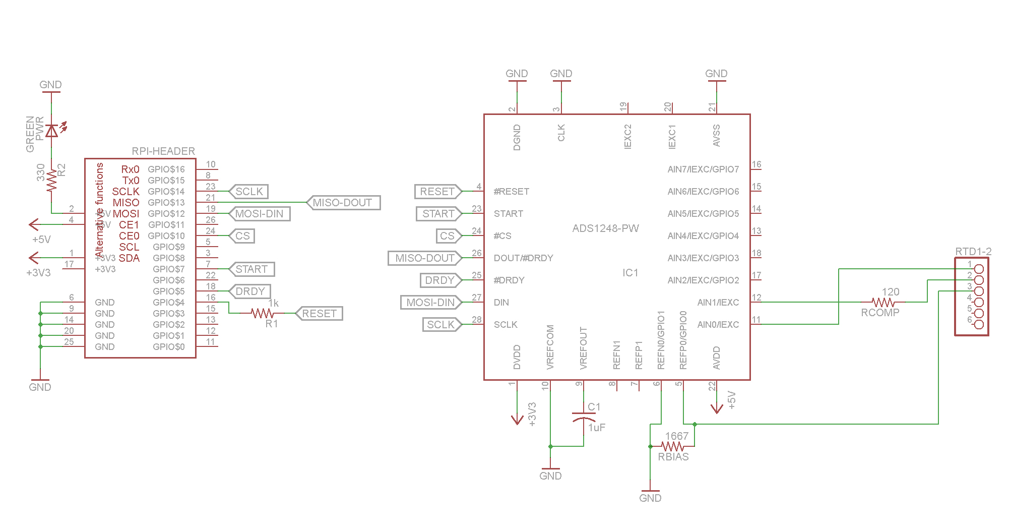
Here are the values I'm using:
R_comp = 119.4ohm (120)
PGA = 128
IDAC = 0.75mA
Vref = 2.5V
R_bias = 1667ohm
Here's the schematic:
Here's the code (Python):
# Set-up script for ADS1248 ADC Converter
# Configures ADS1248 for four three-wire 100ohm RTDs

# --- IMPORTS ---

import sys
import spidev
import time
import RPi.GPIO as GPIO

# --- ASSIGNMENTS ---
#Define GPIO Pins (using board numbering)
START = 7
RESET = 16
DRDY = 18

# --- VALUES ---
#ADS1248 setup values (used for calculating temperature from conversion calculation)
PGA = 128
Vref = 2.5       #In Volts
IDAC = .00075    #In Amps
Ct = 0.385       #PT-100 temp coefficient (ohm / deg C)
r_comp = 119.40

class ADS1248:
    #ADS1248 register addresses
    MUX0 = 0x00
    MUX1 = 0x02
    VBIAS = 0x01
    SYS0 = 0x03
    OFC0 = 0x04
    OFC1 = 0x05
    OFC2 = 0x06
    FSC0 = 0x07
    FSC1 = 0x08
    FSC2 = 0x09
    IDAC0 = 0x0a
    IDAC1 = 0x0b
    GPIOCFG = 0x0c
    GPIODIR = 0x0d
    GPIODAT = 0x0e

    #ADS1248 commands
    WREG = 0x40     #Write to register (0100xxxx)
    RREG = 0x20     #Read from register (0010xxxx)
    NOP = 0xff      #No operation
    RDATA = 0x12    #Read conversion result
    RDATAC = 0x14   #Read conversion continuously

def resetADS1248():
    """ Resets the ADS1248 by pulsing RESET pin LOW and back to HIGH.

    Returns nothing."""

    #Reset the ADS1248 and re-read register
    GPIO.output(RESET, False)       #RESET pin low -> reset
    time.sleep(0.025)
    GPIO.output(RESET, True)        #RESET pin high -> run
    time.sleep(0.025)

    return

def writeReg(reg,data):
    """ Writes one byte to the given register.

    Accepts two integer bytes: register and data."""

    r = spi.xfer2([ADS1248.WREG+reg,0x00,data])
    return r

def readReg(reg):
    """ Reads one byte from the given register.

    Accepts one integer byte: register."""

    spi.xfer2([ADS1248.RREG+reg,0x00])
    r = spi.xfer2([ADS1248.NOP])
    return r

def convert():
    """ Returns ADC conversion from ADS1248. """

    spi.writebytes([ADS1248.RDATA])              #Issue read data once command
    raw = spi.readbytes(3)                       #Read bytes
    spi.writebytes([ADS1248.NOP])                #Send no operation
    print(raw)
    adc = (raw[0]<<16) + (raw[1]<<8) + raw[2]
    print(adc)
    return adc

def initGPIO():
    """ Initializes RPi GPIO settings for ADS1248 interface.

    Accepts no arguments, returns nothing."""

    #Use board pin numbering (as on RPi)
    GPIO.setmode(GPIO.BOARD)
    GPIO.setwarnings(False)

    #Setup pins as output
    GPIO.setup(START, GPIO.OUT)
    GPIO.setup(RESET, GPIO.OUT)
    GPIO.setup(DRDY, GPIO.IN)

    #Set and hold reset pin high
    GPIO.output(RESET, True)
    #Set start pin high to allow communicating with registers
    GPIO.output(START, True)

def printRegs():
    """ Reads and prints all registers of ADS1248."""

    s = ""
    regs = {'   MUX0' : ADS1248.MUX0,
            '   MUX1' : ADS1248.MUX1,
            '  VBIAS' : ADS1248.VBIAS,
            '   SYS0' : ADS1248.SYS0,
            '   OFC0' : ADS1248.OFC0,
            '   OFC1' : ADS1248.OFC1,
            '   OFC2' : ADS1248.OFC2,
            '  IDAC0' : ADS1248.IDAC0,
            '  IDAC1' : ADS1248.IDAC1,
            'FSC0-RO' : ADS1248.FSC0,
            'FSC1-RO' : ADS1248.FSC1,
            'FSC2-RO' : ADS1248.FSC2,
            'GPIOCFG' : ADS1248.GPIOCFG,
            'GPIODIR' : ADS1248.GPIODIR,
            'GPIODAT' : ADS1248.GPIODAT}

    s += "\n--- ADS1248 Register Values: ---"
    s += "\n         dec    binary     hex"

    for key, value in regs.iteritems():
        r = readReg(value)
        s += "\n" + key + ": " + str(r[0]).zfill(3) + "  0b" + str(bin(r[0])[2:]).zfill(8) + "  0x" + str(hex(r[0])[2:]).zfill(2)

    return s

def configureADS1248():
    """ Configures ADS1248 for four-three wire RTDs.

    Accepts nothing, returns nothing."""

    #writeReg(ADS1248.OFC0, 0b00000000);             #Offset calibration reset (pg 45)
    #writeReg(ADS1248.OFC1, 0b00000000);             #Offset calibration reset (pg 45)
    #writeReg(ADS1248.OFC2, 0b00000000);             #Offset calibration reset (pg 45)
    #writeReg(ADS1248.GPIODIR, 0b00000000);          #N/A - GPIO disabled in GPIOCFG
    #writeReg(ADS1248.GPIODAT, 0b00000000);          #N/A - GPIO disabled in GPIOCFG

    writeReg(ADS1248.MUX0,0b00000001)               #Burnout OFF, AIN0 & AIN1 selected (pg 43)
    writeReg(ADS1248.MUX1,0b00100000)               #Internal oscillator, VREF on, REF0, normal operations (pg 44)
    writeReg(ADS1248.SYS0,0b01110001)               #PGA=128, ADC data rate = 10 SPS (pg 45)
    writeReg(ADS1248.IDAC0, 0b10000101);            #DRDY only, IDAC I=0.75mA (pg 46)
    writeReg(ADS1248.IDAC1, 0b00000001);            #IDAC1 -> AIN0, IDAC2 -> AIN1 (pg 47)
    writeReg(ADS1248.VBIAS, 0b00000000);            #VBIAS off (pg 43)
    writeReg(ADS1248.GPIOCFG, 0b00000000);          #GPIO pins are analog inputs (GPIO disabled) (pg 48)


initGPIO()

#Initialize SPI
spi = spidev.SpiDev()
spi.open(0,0)
spi.cshigh=False
spi.bits_per_word=8
spi.mode=1              #For ADS1248 clock dwells low (CPOL=0) and data clocked on falling edge (CPHA=1)

resetADS1248()

print printRegs()

time.sleep(0.050)

configureADS1248()

print printRegs()

time.sleep(0.050)

while True:
    GPIO.wait_for_edge(DRDY, GPIO.FALLING)      #Wait for DRDY
    time.sleep(0.050)
    print("Data Ready")

    v_rtd_gained = (convert()/16777215.0)*Vref
    v_rtd = v_rtd_gained/PGA
    r_rtd = (v_rtd / IDAC) + r_comp
    temp_C = (r_rtd - 100)/Ct

    print "%.4f (V*128)     %.4f (V)     %.4f (ohm)     %.2f (C)    %.2f (F)" % (v_rtd_gained,v_rtd,r_rtd,temp_C,(temp_C*(9/5)+32))

    time.sleep(5)


GPIO.cleanup()
Here's the result of the above code:
--- ADS1248 Register Values: ---
dec binary hex
GPIODIR: 000 0b00000000 0x00
SYS0: 000 0b00000000 0x00
OFC1: 000 0b00000000 0x00
OFC0: 000 0b00000000 0x00
OFC2: 000 0b00000000 0x00
VBIAS: 000 0b00000000 0x00
FSC2-RO: 064 0b01000000 0x40
FSC0-RO: 192 0b11000000 0xc0
GPIOCFG: 000 0b00000000 0x00
FSC1-RO: 018 0b00010010 0x12
IDAC0: 128 0b10000000 0x80
IDAC1: 255 0b11111111 0xff
GPIODAT: 000 0b00000000 0x00
MUX1: 000 0b00000000 0x00
MUX0: 001 0b00000001 0x01
--- ADS1248 Register Values: ---
dec binary hex
GPIODIR: 000 0b00000000 0x00
SYS0: 113 0b01110001 0x71
OFC1: 000 0b00000000 0x00
OFC0: 000 0b00000000 0x00
OFC2: 000 0b00000000 0x00
VBIAS: 000 0b00000000 0x00
FSC2-RO: 064 0b01000000 0x40
FSC0-RO: 000 0b00000000 0x00
GPIOCFG: 000 0b00000000 0x00
FSC1-RO: 019 0b00010011 0x13
IDAC0: 133 0b10000101 0x85
IDAC1: 001 0b00000001 0x01
GPIODAT: 000 0b00000000 0x00
MUX1: 032 0b00100000 0x20
MUX0: 001 0b00000001 0x01
Data Ready
[127, 255, 255]
8388607
1.2500 (V*128) 0.0098 (V) 132.4208 (ohm) 84.21 (C) 116.21 (F)
The first set of register reads is upon chip start up, and the second set is after configuring, demonstrating that I can communicate with the chip and read registers. The issue is that the three bytes read out for the conversion are always [127,255,255].
Thanks in advance for any help you can offer!
