This thread has been locked.

If you have a related question, please click the "Ask a related question" button in the top right corner. The newly created question will be automatically linked to this question.

DAC8734 output buffer

Other Parts Discussed in Thread: DAC8734

Hello,

I am thinking about a unity gain buffer that can drive a 100 Ohm load from the output(s) of the DAC8734. There was a similar discussion going on about a year ago: "Buffer amplifier for DAC8734EVM".


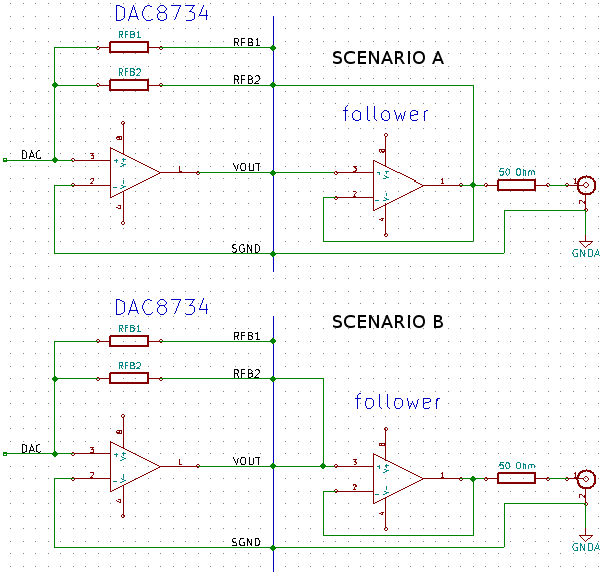
The DAC8734 has got in-built feedback resistors RFB1-x and RFB2-x.

I wonder what would others say about the following two scenarios:

A) use the internal feedback resistor(s) as a common feedback for both amplifier stages (internal + high-current output external)

B) use the internal feedback resistor(s) for the internal amplifier only, followed by a unity gain high-current output external amplifier with its own feedback.

My gut feeling is that A) might give more accurate voltage output. B) might be more stable/reliable.


What do the experienced members think? Has anybody tried either of these scenarios successfully?


Cheers, Jakub

  • Jakub,

    I'm having some difficulty visualizing exactly what you mean in case A. Could you put together some illustration for me to look at?
  • Hello Kevin,

    Thanks for the prompt response and apologies for being so unspecific in my initial post. I quickly sketched a schematics, where the top shows the scenario A, with the follower/buffer in the feedback provided by the internal resistor and the lower schematic B showing the option where the follower would be separate. I hope it makes more sense now.

    My gut feeling is that the latter is the likely to work better, but being not a specialist in analog electronics at all (research scientist at a College) I would like to consult with the community the merits or drawbacks of either approach.

    Cheers,

    Jakub

  • Hello Jakub,

    Thank you for sharing the illustration, your proposal is clear now.

    I would suggest that you stick with your gut and go with the design that is shown in Scenario B. The reason I suggest this is because if you use this approach then the DC voltages that you get at the input to the follower stage will match the specifications shown in the DAC8734 electrical characteristics table since that's how the part was characterized.  If you start with those DC performance figures it will be very easy to calculate the performance at the output of the high-current follower stage.

    Scenario A complicates this a bit because the high-current amplifier in the follower stage is now inside the feedback loop. The amplifiers that you're going to have to choose from that can source higher current are also going to come with higher input offset voltage. The input offset voltage of this follower stage is now within the feedback loop and will interact with the trans-impedance circuit inside the DAC (the internal amplifier plus feedback resistor) and create a sort of modulated representation of Vos at the output based on the input code to the DAC, in short a linearity error that you wouldn't have had if you used Scenario B. There is a reference design that explains some of this that you can refer to here.