This thread has been locked.

If you have a related question, please click the "Ask a related question" button in the top right corner. The newly created question will be automatically linked to this question.

ADS1299 with Arduino Sampling problem

Other Parts Discussed in Thread: ADS1299

I have EEG Front-End Performance Demonstration Kit and got clear idea bout the operation of the chip. 

Then I decided to use ADS1299EEG-FE Daughter Card separately with Arduino DUE.

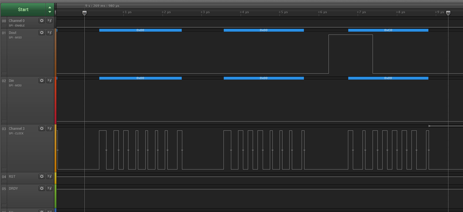
Then I made all the necessary connections(SPI , Reset, Start, DRDY) between Daughter Card and Arduino. The required power (3.3V and 5V , GND) are supplied from Arduino board.

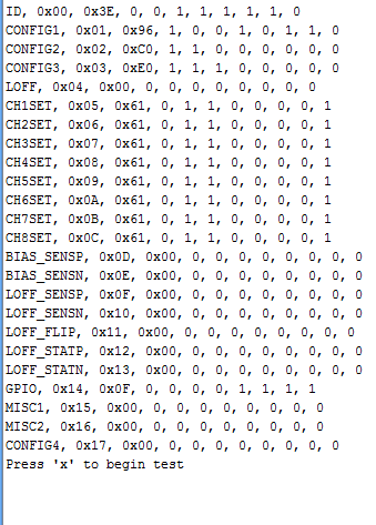
When I run the program it shows the default register values correctly as follows. That implies the chip powered up correctly 


Then I Modified CONFIG3, CONFIG1, CH1SET   registers to apply TEST signal to CH1 and take 250 samples.

Case 1 : START pin is connected with  CS pin using JP22 of the Daughter Card

The problems comes after this.

  1. It takes 4026 ms to take 250 samples. This is unusual time since the default sampling rate = 250 SPS. Then I assume the sampling rate is less than 250SPS


  1. When I plot the graph I do not show the square wave pattern as I expected.(I think due to low sample Rate)


Then I apply Small Sine signal externally To CH1 from a signal generator. ( Vpp= 10 mV , f=6 Hz)

This signal show on the graph correctly. But when the frequency of the signal increases above 10 Hz, the graph start to distorted .

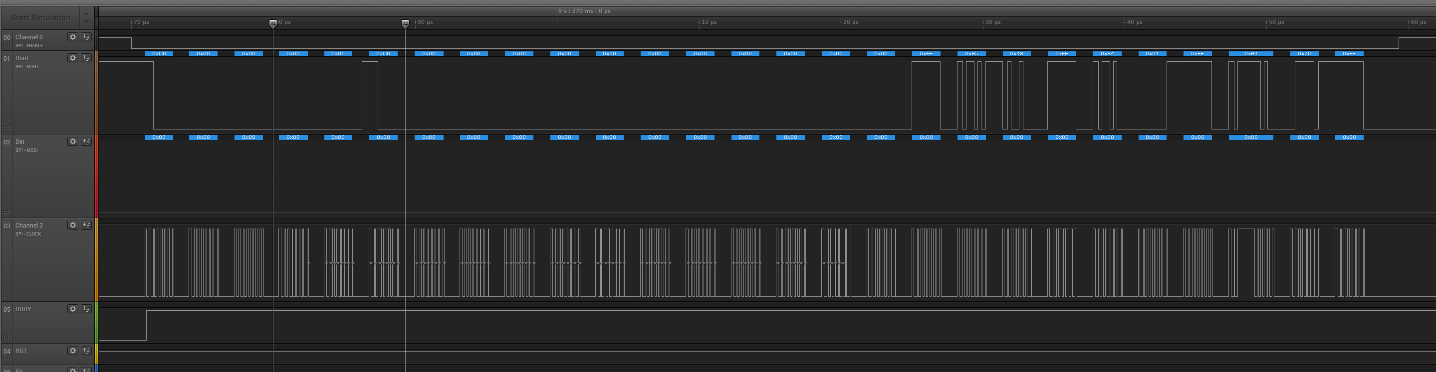
Case 2 : START pin is directly connected to GND

  • At this time It take only 1322 ms to take 250 samples which is a reasonable time . But the problem is I don’t observe the correct Square wave form from the channel.


The waveform is in this graphs but there are un expected peak values (errors) ..

Sometimes the graph shows almost correct with small level of error values as follows


According to the manual START pin should be grounded 

Please help me to correct this. I think I’m almost done but stuck at this point. 

  • Hey Vibodha,

    There are a couple of issues with your setup that I see that could account for some of the strange behavior you are seeing. 

    First, tying the START and CS pins together is not a valid configuration. I believe that the collections might be taking so long because you are restarting the converter every time the device is addressed by the host. The distortion over 10 Hz may be explained by the reduced effective sample rate imposed by the delay between conversions. If you intend to start conversions using the START commend, which it seems from your second case that you are doing, then you can just tie the START pin low. 

    The strange errors you are seeing in the output waveform might have something to do with the SPI communication or how the data is handled following acquisition. I’d start by verifying that your data collection SPI transaction matches the format described in the ADS1299 datasheet. You can take a look at the data with an oscilloscope or logic analyzer to see what is happening. If that looks good, trace through your code to see what could be happening to it at each step before you see it in the graph.

    Regards,

    Brian Pisani

  • Dear Brian,

    Thank you for the response....

    Today I did some experiment with it...

    First I power down all the channels by assigning CHnSET = 0x80 to all the Channels and got Zero for each channel as expected.

    Then I set the CH1 to the test signal configuration while keeping the others Power down Mode.. Then I got nice Square form.. I got samples for several times and got the correct result as follows. This worked for each an every individual channel while other keeping power down mode.

    Then I added other channels one by one to the test signal mode and got correct result until Three channels set to test signal while others in power down mode. When a 4th channel set to Test signal , I observed unexpected results. 

    Here CH1, CH2 , CH3,CH4 are in Test Signal mode.. CH5-CH8 are in power down mode. CH1-CH4 shows Square wave correctly. CH5- CH8 are must be in Zero level. but this is what I got

    CH5

    CH6

    CH7

    Then I added CH5 to the test signal  ( CH1,2,3,4,5 = Test signal        CH6-8= power down)   ..

    Now CH1,CH2,CH3,CH4, CH5 started to distort. 

    CH1

    CH2

    CH3

    CH4

    And the power down channel are not in the zero level also...

    There were no problem with any three channels apply to the test signal..If I add a 4th channel, all the errors going to be appearer..  

      Where should be the problem ?? 

  • Hey Vibodha,

    It is typically a challenge to get the communication working for collecting data from multiple channels. I would recommend you check your SPI communication with an oscilloscope or a logic analyzer to ensure the collection routine is happening as you expect for all the channels. If the communications look clean, take a look at how the data gets manipulated in your firmware. Perhaps there is some sort of data corruption going on with your firmware that you don't expect.

    Regards,
    Brian Pisani
  • Thanx Brian ,

    The thing I don't understand is why this happens after adding 4th channel..Ok i'll check the SPI signals .

    As a side note : I'm using the OpenBCI ADS1299 library for arduino DUE.

    Thnak you
  • Dear Brian,

    Today I analysed SPI Lines using a logic analyser. The raw data observed from the SPI Analyser is same as the data I observe from the graph. i.e the error samples shown from the output  graph also shown in the raw data. I think this implies there is no data corruption after the acquisition.

    Here CH1 is in power down mode and acquired 200 samples and 187th sample has error value. The hex value of the sample is C0.

    This values shows in the SPI raw data observed from the analyser as follows


      ie. I have received corrupted data from the chip. then how to fix it?? When I connect the daughter card to MMBO board,  it works fine... 

    I need to overcome this problem.. Brian Pisani  please assist me.. 

  • Hey Vibodha,

    Is that value 0xC0 the most significant byte of one of the channels? That value also happens to be the first byte one would expect to receive for the 24-bit status word. Also, looking more closely at the picture of your good data, the magnitude does not seem to be correct. Could you kindly take a picture of the entire transaction from when DRDY falls low to when the the final channel's data has been shifted out of the device?

    Thank you,
    Brian Pisani
  • Hi Brian,

    No. 0XCO is the Least significant byte out of three bytes of Channel as the image.  All the other data points of the channel is on Zero level except this point. The magnitude of the graph is different from 0XC0because C0 is converted to 32 bit sign value since data coming in 2's compliment format from the chip. 

    since 0000C0 is positive value the signed magnitude is =192 

    Yeah I will put full image after couple of hours because I'm out of the lab. 

    Again thank you very much for your response Mr.Bran

    vibodha 

  • Hi Brian Pisani,

     This is the capture of effected sample ( Sample no 187)

    This is the capture of  unaffected sample( Sample no 186)

    Thank You 

    Vibodha

  • Hey Vibodha,

    That is very strange behavior. At this point I cannot explain why it is happening, but I think I understand what is happening. The value of 0xC0 on that seems to occur on the first channel is not trivial. As I mentioned before, 0xC0 is the first byte of the status word. In the case of sample number 187, look at the SPI transaction and imagine that second occurrence of 0xC0 is actually the beginning of the status word. If you do that, you's see channel 1 = 0x000000, channel 2 = 0x000000, channel 3 = 0x000000, channel 4 = 0xFEB548, channel 5 = 0xFEB401, channel 6 = 0xFEB47D, and channel 7 starts as 0xFE but is cut off by the end of the transaction.

    If you look at sample 186, you'll find the numbers I've just proposed to be very similar. I am not certain what could be causing this, but I have a theory. It is clear that something is causing the interface to reset during the middle of your sample 187 acquisition. There could be too much time between when DRDY falls low on sample 187 and when collection actually begins. If the the next DRDY falls low during acquisition, the device will just start to shift out the new data immediately. How much time passes between when DRDY falls low and SCLKs begin for sample number 187? We cannot see DRDY fall low on the logic analyzer, but perhaps it happens so fast that the analyzer misses it. The reason it would happen on only sample 187 is perhaps the delay between when DRDY falls low and when collection occurs increases a little bit every sample until sample 187 where it finally disrupts a collection.

    Regards,
    Brian Pisani
  • Hi brian,

    The thing that you are saying can be true because only CH1,CH2,CH3 are in power down mode.. CH4- CH8 in test signal mode.. so in sample 187 , CH4 value is 0x00 which no true . Here is the graph of CH4 with square wave form and at sample 187 have unexpected Zero value..

     The time passes between when DRDY falls low and SCLKs begin for sample number 187 = 3.099 ms

    Thank you very much

    vibodha


  • Dear Brian,,
    Problem solved.....
    In my program I had sent each an every sample to serial port as it collected....This should have caused the delay for obtaining samples.....

    Now I collect all samples and stored in a 2D arry. then send data to the serial port... now there is no errors...

    Thank you very very much for your great help with your knowledge...

    Vibodha
  • Hey Vibodha,

    Glad I could be of assistance.

    Regards,

    Brian

  • hi,

    I am trying to record EEG data with the help of ADS1299 and Arduino board. i can read register initial value but I am unable to record any signal. Could you please share your code. so, that I can use it.

    Thanks,

    Rinku

  • hy very sory for the late reply... i used libraries from open bci... pls do mail me vibandara@gmail.com . i'll try ro help you.

    thank you.
  • Sir, I have done the set up of ads1299 registers but not able to do the main program code for getting data.
    i didnt even understand C0 hex .
    i have used open bci code in arduino uno .
    I want to know how i have to do the coding to get data through all channels