This thread has been locked.

If you have a related question, please click the "Ask a related question" button in the top right corner. The newly created question will be automatically linked to this question.

ADS1298 AC interface problem .

Other Parts Discussed in Thread: ADS1298

Hello 

We are using ADS1298 in our product ; 

The problem is the AC  line interface that distroy  completely most the times or  add noise to the ECG signal ; Even we have the sigital filters nortch  in the DSP side. 

May it is the RLD problem ; but we use the values suggested by TI 1.5nF with 1M ohm on the feedback that gives about 106 hz , 

So please could you guide us to solve this problem; here the pictures of the ECG 

When the device is powered from battery the first picture as you see a good ECG ; but when we power the system from AC  ;  the ECG is noisy and some times is gone completely ;  even we use isolation power between the main board (DSP ) and the analog  side ADS1298.
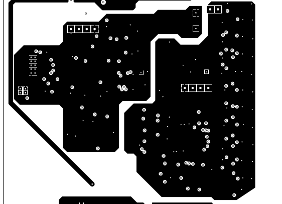
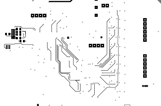
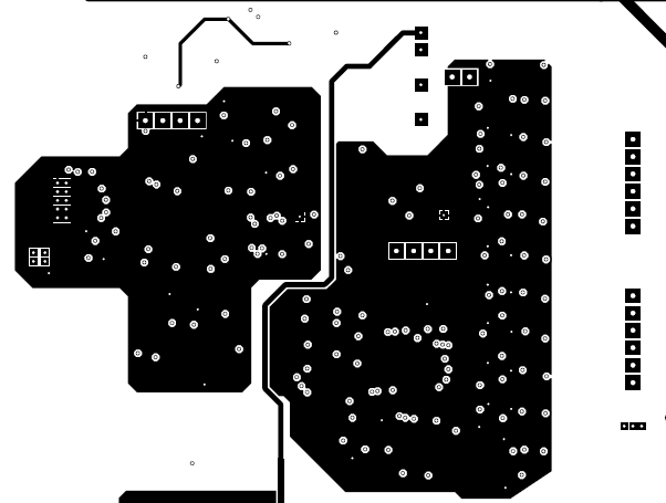
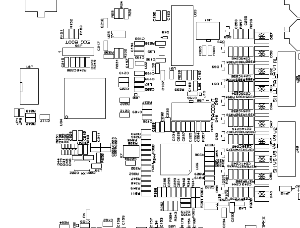
Here our shematics 

ads1298.pdfads1298_2.pdfads1298_power.pdf

Thank you ; 

Regards 

  • Hello Hector,

    Looking at the schematic, your input anti-aliasing filter has an extremely wide bandwidth (~35 kHz). That will allow wide band noise to couple into the inputs to the ADC which may introduce unwanted aliasing near multiples of the modulator frequency. What is your expected signal bandwidth? ECG signals typically have a bandwidth <= 50 Hz. I'd recommend narrowing the passband of your input RC filters as much as possible.

    In addition, have you characterized the noise that you are seeing? How can you be sure the distortion is because of the utility noise? Also, what is the response of your notch filter? What sort of attenuation do you expect right at the utility frequency and a few Hertz on either side? The utility frequency tends to drift a few Hertz from its nominal value so the response of the filter at nearby frequencies may be important to characterize.

    Regards,
    Brian Pisani
  • MATLAB.pdfHello Brain ;

    First Thank you for the support ;

    since we detecting the PACE too ; so our  ECG bandwidth is  about 2khz ; our sampling freq is 8k ; so what is the suggested anti- aliasing filter here ?   for that  what is suggestted  to increase the capacitor of the filter  or the resistor ?

    for the  AC filter we are using  300 tab FIR ; bandstop filter 48 to 52 ;  least squres 300 tab ;we   sample at 8k but we get the ecg at 250 sps we use DECIMATOR  of 32 .

    When we use the simulator with AC powered or when we power the system from AC we get this propblem ; so we think it is an AC probelm we need to solve it. Any suggestions from you would be very helpful for us . 

    Thank you 

  • Hey Hector,

    If you had a filter whose magnitude response at 2 kHz was roughly -2 dB, that should be enough to preserve your band. The goal of this filter is to have significant attenuation around 512 kHz since that is where the alias of the digital filter will appear. In terms of what resistors and capacitors, it shouldn't matter too much now big they both get. The easiest approach to choosing will probably just be to simulate a Bode plot with different values so you can see what kind of bandwidth you get from different combinations. There is an equation for the response to a two pole RC LPF, but calculating the response for different combinations by hand would likely be tedious. In general, however, the larger both the resistors and capacitors get, the lower the bandwidth will be.

    The one thing you may run into is if your diodes tend to leak current then the IR drop across the resistors could cause an offset at the input to the ADC. If you know how much current will be drained by the diodes, then you can predict what kind of offset you will get from whatever resistors you chose for your RC filter.

    That filter response looks pretty good, but I'm still unclear on a couple things. How are you detecting a pacemaker? Are you sending the signal from the PACEOUT pins to another data converter? If that's the case and you never use the ADS1298 modulator to detect the pulse, then why keep the data rate so high? This device is capable of digitally filtering and decimating as low as 500 SPS in high resolution mode. In that case, you would only have to decimate by a factor of 2 to get an effective 250 SPS data rate.

    In your decimation routine, are you low pass filtering the signal to reflect a lower Nyquist rate? If you are simply removing points, you are likely to alias all signals which were in band for the ADS1298 digital filter but would not be in band for a 250 SPS data rate. Then I could see the noise being attributed to aliased utility frequency harmonics (i.e. 100 Hz, 150 Hz, 200 Hz, etc.).

    Regards,
    Brian Pisani
  • Hello Brian ; 

    I will change the input filter to about 1khz by combining  10k with 1.5nF. I will remove the diods from teh circuit. 

    For pace maker we are detecting it by software so we are sampling at 8khz ; the other aim of sampling at 8khz to also we detect R to syncronize the ECG signal with other system . 

    what we are doing exactly is  we  removing  31 points and getting the 32 point ;  then  we apply 52 tab fir low pass filter of 100 hz ; 

    then we apply the 300 tab AC filter ; so do you mean we should have do the filterring  first then remove the points ? 

    We noticed that some some people use RLD circuit in diffirent way ; but I could dont understand how  does it effect the system 

    rldrive.pdf

    Any comments for this RLD drive circuit? 

    Thank you Mr Brain 

    Regards 

  • Hey Hector,

    I think my confusion stems from the following question. If you are sampling fast in order to capture a pacemaker pulse, why decimate? You will likely lose the pulse. Are there different processing steps for your pacemaker detection channel?

    And yes it is critical that low pass filtering happens pre-decimation since if you decimate first, then all the out of band information will alias into the newly established Nyquist band and the effect of the low pass filter is mostly lost.

    Before continuing with the RLD amplifier analysis, are there any bits set in the RLD_SENSP/N registers? If there are not, then I seriously doubt the RLD feedback configuration is causing the issue since no small signal will be driven to the input of the amplifier.

    Assuming you are using input voltages as feedback for the RLD amplifier by setting corresponding bits in the RLD_SENSP/N registers, I simulated the responses of the proposed circuits. Looking at your proposed circuit in simulation, you essentially seem to be reducing the gain-bandwidth product of the RLD op-amp by increasing the size of C219 in the feedback circuit. Through simulation I measured the GBW product of this configuration to be 70 Hz. This is low considering the RLD op-amp is in a negative feedback topology and the circuit aims to cancel a 50 Hz signal by sending an inverted signal back to the body. In the configuration recommended by the datasheet, the GBW product is 475 Hz which provides plenty of bandwidth to cancel a utility signal on the body.

    That being said, since you only observe the phenomenon when the circuit is powered from the wall, it makes me think that the noise is coming from somewhere on the board since if it were coupling on through overhead lights or by some other means, you'd expect the noise to appear even when the circuit is battery powered. Would you mind sending me your layout to review?

    Regards,
    Brian Pisani
  • Hi Brain ; 

    Thank you for your effort ; 

    We sample at 8khz we proccess the pacemaker routine at 8khz ; then we decimate to 250Hz ( after decimate) we process LPF, DC filer an norch filter. 

    As I understand from you ; we should first apply the  LPF  then decimate, after that DC filter and norch filter ; Am I right? 

    for RLD ; 

    here my registers 

    //CONFIG1 0x0001
    0x82,
    //CONFIG2
    0x10,
    //CONFIG3
    0xDC,
    //LOFF
    0xFF,
    //CH1SET (PGA gain = 6)
    0x00,
    //CH2SET (PGA gain = 6)
    0x00,
    //CH3SET (PGA gain = 6)
    0x00,
    //CH4SET (PGA gain = 6)
    0x00,
    //CH5SET (PGA gain = 6)
    0x00,
    //CH6SET (PGA gain = 6)
    0x00,
    //CH7SET (PGA gain = 6)
    0x00,
    //CH8SET (PGA gain = 6)
    0x00,
    //RLDSENSP (default)
    0x06,
    //RLDSENSM (default)
    0x02,
    //LOFF_SENSP
    0xFF,
    //LOFF_SENSM
    0x02,
    //LOFF_FLIP (default)
    0x00,
    //LOFF_STATP (Read only)
    0x00,
    //LOFF_STATM (Read only)
    0x03,
    //GPIO
    0x00,
    //PACE (default)
    0x00,
    //RESP (default)
    0x00,
    //CONFIG4
    0x02,
    //WCT1
    0x0A,
    //WCT2
    0xE3,

    //--

    SO I use 0x06 for RLD_P ; we routes only  LL and LA ;  here what is the advantage or disadvantage of routing more channles ? 

    The circuit I posted last for RLD with 10nF and 10k series ; do you mean this circuit BW is 70hz ? Is that better circuit from that one of teh datasheet ? I mean here is it better for the 50hz noise ? 

    for the layouts please check the pictures ; 

    Regards 

  • Hi Brain ; 

    Thank you for your effort ; 

    We sample at 8khz we proccess the pacemaker routine at 8khz ; then we decimate to 250Hz ( after decimate) we process LPF, DC filer an norch filter. 

    As I understand from you ; we should first apply the  LPF  then decimate, after that DC filter and norch filter ; Am I right? 

    for RLD ; 

    here my registers 

    //CONFIG1 0x0001
    0x82,
    //CONFIG2
    0x10,
    //CONFIG3
    0xDC,
    //LOFF
    0xFF,
    //CH1SET (PGA gain = 6)
    0x00,
    //CH2SET (PGA gain = 6)
    0x00,
    //CH3SET (PGA gain = 6)
    0x00,
    //CH4SET (PGA gain = 6)
    0x00,
    //CH5SET (PGA gain = 6)
    0x00,
    //CH6SET (PGA gain = 6)
    0x00,
    //CH7SET (PGA gain = 6)
    0x00,
    //CH8SET (PGA gain = 6)
    0x00,
    //RLDSENSP (default)
    0x06,
    //RLDSENSM (default)
    0x02, 
    //LOFF_SENSP
    0xFF,
    //LOFF_SENSM
    0x02,
    //LOFF_FLIP (default)
    0x00,
    //LOFF_STATP (Read only)
    0x00, 
    //LOFF_STATM (Read only)
    0x03, 
    //GPIO
    0x00,
    //PACE (default) 
    0x00,
    //RESP (default)
    0x00,
    //CONFIG4
    0x02,
    //WCT1
    0x0A,
    //WCT2
    0xE3,

    //--

    SO I use 0x06 for RLD_P ; we routes only  LL and LA ;  here what is the advantage or disadvantage of routing more channles ? 

    The circuit I posted last for RLD with 10nF and 10k series ; do you mean this circuit BW is 70hz ? Is that better circuit from that one of teh datasheet ? I mean here is it better for the 50hz noise ? 

    for the layouts please check the pictures ; 

    Regards 

  • For more info ; we put the osc. on the RLD we noticed it is very noisy with +/- 1v 50Hz over 1.6Dc volt=( 3,3VADD/2).
    when the ECG is ok it is the RLD is 1.6DC ; but we could not find the source of the this noise ; we have tried all the RLD compinations ;
  • The last status of the project : 

    When getting the ECG from the simulator and the simulator is powered from the battery . GOOD ECG signal 

    when I powred the simulator from 50hz AC line . no ECG very bad signal 

    when I connect  the to human body also we get no ECG very  bad signal ;

    it seems  it is common mode rehection problem ;  may be the RLD probelm or any other thing from the circuit we still miss .

    Any suggestions ?

  • Hey Hector,

    I’m sorry I wasn’t clear before about the DSP algorithm I was suggesting. The ordering of the filters will depend on what effective sample rate you’ve built the filters for. Here’s what I recommend:

    Collect data at 8 kSPS (use data to do pacemaker detection algorithm) → LPF data with 100 Hz cutoff → Decimate by 32 (new effective sample rate is 250 SPS) → Apply DC blocker and 50 Hz notch

    From what I understand about your system, you’ll likely have to design a new 100 Hz LPF since the one you have now has a cutoff of (100 Hz/250 Hz)*2π rad/sample = 2π/5 rad/sample in normalized frequency. If you were to apply a filter with that cutoff to samples that had a sample rate of 8000 Hz, you’d get a cutoff of 3200 Hz. All of your other filters were built with the 250 SPS sample rate in mind so I think those will be fine.

    The function of the RLD amplifier in the configuration you have it is to cancel any common-mode signals that appear on the body by applying the inverted common-mode signal to the body. With the RLD_SENS settings you have, the amplifier will take any signals that appear common on the RA, LA, and LL electrodes, invert and gain them, and apply that signal to the body to cancel it. This is a valid configuration.

    In general, the wider the bandwidth on the RLD amplifier, the better it will perform since it will allow the amplifier to cancel wider band common-mode signals. The datasheet configuration with a GBW product of 475 Hz will, in theory, provide more effective cancellation of a 50 Hz signal than an op-amp configuration with a GBW product of 70 Hz. That means the datasheet configuration should perform better.

    To test whether or not there is some sort of ringing going on with the RLD amplifier, try setting both of the RLD_SENS registers to 0x00. This will essentially turn the RLD amplifier into a unity gain buffer. If the problem was stemming from ringing on the amplifier, that problem will disappear or at least improve significantly.

    When I asked for you layout files in my last post, I apologize since I was under the impression that you were seeing the noise when your board was powered from the wall rather than the simulator being powered from the wall. If it is only the simulator being powered from the wall or when you connect electrodes to the body, then it is extremely likely to be a common-mode rejection issue. The issue could stem from component mismatch on the input signal path (i.e. RC filters, cable mismatch, etc.). Check out this document on sources and ways to mitigate poor common-mode rejection performance: http://www.ti.com/lit/an/sbaa188/sbaa188.pdf

    Let me know what you find out through further testing.


    Regards,

    Brian Pisani

  • Hi Brain ;

    For the test for RLD ; I set both RLD_SENS to 0x00 the signal shape is changed still not ok but improved and still noisy ; the software here is changes ; we sample at 500sps ; we do all the filterring at 500sps the decimate to 250;

    here 3 pictures of ECG ; the first with  simulator being powred from battery ; the ECG is good

    the second powered from AC with RLD_sens _regesters routed to the leads .

    the thirst AC powred with RLD_sens registerd =0x00.

    What do you mean by ring ?

    For the second test  related to the common mode I will give you the results tomorrow .

    Thank you Mr Brain 

    Regards 

  • Hey Hector,

    When I say "ringing" I'm referring to amplifier stability. If the amplifier was driving a large capacitive load, then its possible for it to become unstable and oscillate. The only significant source of capacitance that I can think of on the path of the RL electrode is the cable. It looks like you are using the RLD amplifier to drive the cable shield. Out of curiosity, would it be possible to connect the cable shield to ground and depopulate R364? It would be interesting to see if that shows improvement.

    Regards,
    Brian Pisani
  • Hi Brain ;
    We did that but no any success .
    Tomorrow we will check the test for common mode ;
    what things would effect common mode ? the cables ? the pcb ? Do you think our layout is ok ? power supply ?
    because that is really strange thing we have it here on the office .
    Thank you Brian
    Regards
  • Hey Hector,

    That document I linked to in a previous post has some great explanations on the sources of common-mode rejection degradation. To test it, you can short the inputs and generate a common signal and see what the magnitude of that signal is at the output. That method would be good since it does not involve the RLD output so we can see how much the input mismatch is contributing the the poor input common-mode performance.

    Regards,
    Brian Pisani
  • Hi Brain ;
    First I would like to thank you for your effort ,
    we changed the chip ADS1298 with other one ; and it works now as expected ; it seems that RLD out is being failled for some reaons may be during soldering . I approciate your help to us thank you .
    In our system the leads will be selected ; 3 leads cable(3 electrodes) , 5 leads cable and 12 leads cable ( 10 electrods), how does that effect the configeration of the ADS1298 ? Do we need only to change the configurations of RLD only ?

    Regards
  • Hey Hector,

    I'm glad it's working now! You're right; all you'd have to do is set those bits in the RLD_SENSP/N registers corresponding to the electrodes which are connected to the body for the best performance on the RLD amplifier.

    Regards,
    Brian Pisani