This thread has been locked.

If you have a related question, please click the "Ask a related question" button in the top right corner. The newly created question will be automatically linked to this question.

ADS1299 noise level under Internal input short

Other Parts Discussed in Thread: ADS1299

Hello, 

  For ADS1299 internal input short condition, which both inputs of PGA be (ADSS+AVDD)/2 by setting register value MUX[2:0], 

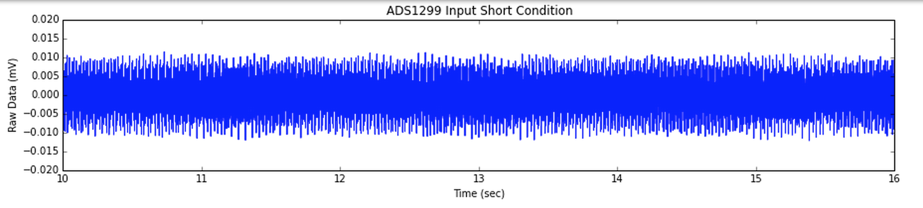
As seen below, I'm getting ~1uV on ADS1299 EVM with power supply in bi-polar (+-2.5V). 

And, corresponding register settings are, 

 However, on our developed board with same exact register setting as above, I'm getting ~20uV of noise level. 

 [Raw data plot is attached below] I believe it picks up ECG pretty successfully, but not EEG. (guess it's due to high noise level). 

I think we met pretty much all the PCB design criteria / requirements for successful EEG signal acquisition, but I have no idea where does that amount of noise is coming from ?

On page 3. of ADS1299 Data sheet, Offset error is specified as 60uV. I wonder if that 20uV can be the offset error.

Then, Does ADS1299 EVM plots raw data without offset ? 

Can anyone comment on this ? Thank you.

  • Hey Jason,

    Offset is defined as the DC value when the inputs are shorted and RMS noise can be defined as the average distance away from that DC value. From a statistical perspective, you can think of the offset as the "mean" data value and RMS noise as the "standard deviation".

    In the data you collected from the EVM, the offset can be identified roughly as the location on the vertical axis which each of those different channel plots sit and the peak-to-peak noise is the peak distance from the smallest to the largest voltage on any channel.

    In the plot you've gathered from your design, the offset is stationed at zero and the noise looks to be roughly 20 uV. First, is that data input referred? The noise specifications in the datasheet (and the plots on the EVM) are defined as input referred; meaning the measurement values were divided by the PGA gain. It looks like you are using a PGA gain of 12. If you were to divide the 20 uVpk-pk noise by the PGA gain, you'd get 1.67 uVpk-pk, which is very close to the datasheet typical specification for that gain and data rate. Out of curiosity, are you removing the DC offset from the data or is it coming out of the device centered around zero?

    If the data you've plotted is input referred, then one possible source of the noise is the reference. Since the inputs are internally shorted, it is not possible that noise could be coupling to to the device from the inputs. I notice you are using the internal reference. I wonder if the reference pins have the proper decoupling. If you are sure that the data you've collected is input referred, would you mind attaching your schematic and layout here for me to take a look at?

    Regards,
    Brian Pisani
  • Brian,

    I do appreciate for your kind support.

    First, when internally shorted, increasing PGA gain puts more higher noise (not sure if it really is noise). So, I will check more closely, and let you know if it is input referred. Then, If I set PGA gain to 1, then would I get ~1uVpk-pk of noise level ?

    And, for your question, I removed DC offset from the data with high-pass filter after raw data. And, the data is coming out of the device centered around zero.

    Secondly, can you let me know your email address? I would appreciated if you can go over our schematic and PCB design. If you are okay, please let me know what file format would be good for you. I think we followed pretty much all the recommended designs requirements, but you will find more details on the schematic.

    Thank you.
  • Hi Jason,

    At Gain = 1, I would expect to see about 11uVpp with a data rate of 500SPS. You can refer to the noise measurement tables on pages 6-7 to see how input-referred noise is affected by PGA gain.

    I will follow up with an email and review your schematic/PCB layout.

    Best Regards,