


Other Parts Discussed in Thread: DAC8568
I'm driving a DAC8568 (A grade) with an FPGA (and therefore every change I make requires some tens of minutes for the firmware recompiling). I can't make it work and I don't understand why, so before starting a very time-wasting trial and error process I'm trying to get some hints. This is a typical trace with three commands:
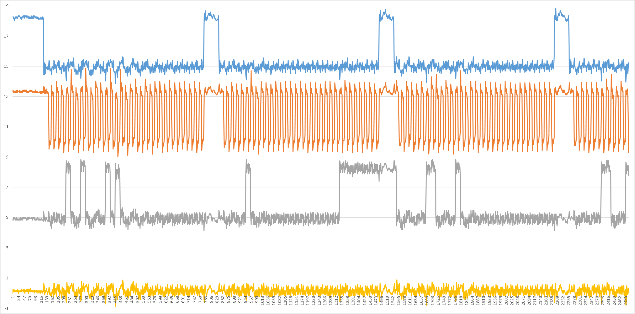
Blue is SYNC#, orange is SCLK, gray is DIN and yellow is LDAC# (always low). The clock frequency is 25 MHz.
The first command is 0x090A0000 which enables the internal reference. This works, I can see the 2.5V pop out from the vrefout/vrefin pin.
The second command is 0x040000FF which should power on all the outputs.
The third command is 0x03080000 which should immediately set the first output to midscale, i.e. 1.25V for the A grade. After that there are seven similar commands for the other seven outputs (not shown).
Everything looks good, but all the outputs are stuck at 0V. Why?
Thanks!

