This thread has been locked.

If you have a related question, please click the "Ask a related question" button in the top right corner. The newly created question will be automatically linked to this question.

ADS1672 Input part question

Other Parts Discussed in Thread: ADS1672

Dear Sir,

I am planning to design the circuit to change the input range (0 ~ 3.2V) with ADS1672. Here’s the history.

Input range is as below 2 item, which was written in the data sheet ADS1672.
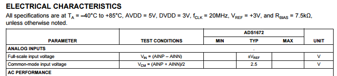
Q1) Could you let me know how to choose Full-scale input and Common-mode input?

I assume that Full-scale input fits to the above purpose.  Personally, whether VCM PIN is used or not is the key point.

Is it right? If it’s not, Please let me know how to choose.
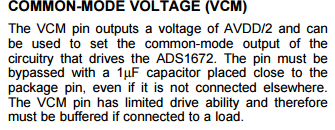
 

Q2) When designing the circuit of input terminal, I wonder if the circuit recommended in the data sheet has to be used.

For the main purpose, I designed the circuit. Please take a look at the below image and feedback me.
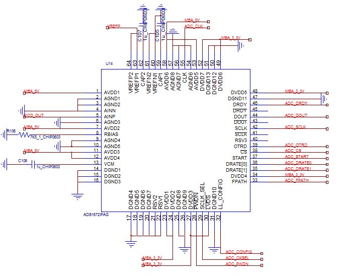

CCD_OUT  =  Input Voltage (0 ~ 3.2V) 

ADC_CLK  =  Clock supply through 20MHz Oscilator. 

Vref = Datasheet has to be used.   

AVDD1~6 = 5V(=MB_5V) supply through LDO Circuit (using TPS79901)

DVDD 1~7 =  3.3V(=MBA_3.3V) supply throgh LD0 Circuit(using TPS7A4700)

Thanks and regards,

  • Hello Kim -
    The full-scale input of the device should be set based on your input signal. If your input signal is larger than your full-scale range, you will clip the ADC output code (see Table 9 in the datasheet).
    Since the ADS1672 does not have a built in PGA/buffer, you need to buffer the input signal. The examples shown in Figures 40 and 41 of the datasheet are references that provide a suggested way to achieve the buffering. These circuits are not the only solution, there are potentially many more that may suit your circuitry and system better based on your requirements.
  • Hello Greg -


    Thank you for answer quickly.

    I have your answer on the question.

    Q ) If you do not have a buffer, What is the problem?
         >> I wonder what is the main function of the buffer.
        >>  Is there a problem when converting an input voltage(0~3.2v) from the current circuit status?


    Thanks and regards,

  • Hello Kim -
    The buffer provides current to charge the switched cap input of the ADC. Without the buffer, the input capacitor may settle correctly and provide an error in the voltage conversion.
  • Hello Greg -

    Thank you for answer quickly.

    ADS1672  Inuput Voltage(0 ~ 3.2V ) is  output voltage of the single differential amplifier circuit.

    Brief description about single differential amplifier cicuit .

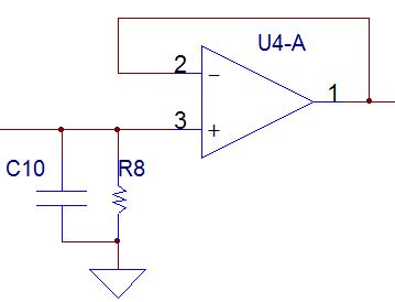
    Vs-  = 0v, VS+ = 5V, Vin +  = 2.2V , Vin- =  2.18 ~ 1.18V  Amplification ratio = 3.12

    Vin- input part  circuit

     Output Voltage Range : 0.06 ~ 3.18V 

    So, If seen from function of the buffer, I think this circuit is that function of the buffer a little.

    I want to receive your advice.

    Thanks and regards,

  • Hello Kim -

    Yes, you can use a single ended buffer if desired.  However, ensure that the signal is within the limits of the supplies; you may have to offset the signal from zero volt reference.  We would recommend you keep the anti-aliasing filter and differential capacitor shown in Figure 39.  They help provide charging for the switch cap input stage and filter out any higher frequency components that can alias back into your band of interest.

    Additionally, you need to ensure the bandwidth of your amplifier is adequate.  You might want to reference https://e2e.ti.com/blogs_/b/precisionhub/archive/2014/09/05/do-i-always-need-an-amplifier-to-drive-my-sar-adc or some of our other apps collateral locate at http://www.ti.com/lsds/ti/analog/dataconverters/learning_center.page