This thread has been locked.

If you have a related question, please click the "Ask a related question" button in the top right corner. The newly created question will be automatically linked to this question.

ADS131E08 difference between reset command and reset pin.

Other Parts Discussed in Thread: ADS131E08

Hello,

Is there a difference between the Software Reset command and the Reset Pin. I use several ADS131E08 parallel. Sometimes if I power the device one of the ADS131E08 don't react. All the ADS131E08 get the same configuration commands.

1. start external converter clk until the FPGA is initialised (after power up the System 20 Seconds later the FPGA will initialised )

2. Send reset Command

3. wait more then 18 tclks

4. SDATAC

5. Change config Register 1 set 24 bit mode

6. Set RDATAC

7. Set start pin 1 to synchronise the Converters

8. Wait for DRDY low on all Converters. In this states happens that the one converter doesn't answer. And this behave is random. That means it is ADS131E08 number one, tow three random too. 

After DRDY not react the FPGA try to reinitialise the ADS131E08 again without success.

Can in this Case a the reset Pin help?

The reset pin is at the moment not connected(to connect this is possible, but not provided at the moment) but I should know is the reset pin able to bring the ADS131E08 back to service, even when the ADS131E08 is in a undefined condition.

Best regards

Bernd


  • Hello Bernd -

    The RESET pin and software RESET perform the same behavior (see page 34 of the datasheet).

    For startup reference, make sure that you are following the start-up process shown in Figure 23 of the datasheet.

    For synchronized converters, make sure that you are using the same clock for all ADCs and the same START pulse to synchronize them.  FIgure 46 of the datasheet shows an example of the timing.

    One additional note:  If you are using the daisy chain feature for multiple devices, please ensure that you are taking into account the extra SCLK between device data (see notes at the bottom of page 44 and Figure 48 of the datasheet).

  • ADS131E08 - Unstable DRDY behavior.

    Hello Greg,

    thanks for your support. Unfortunately I have still not solved this big problem with the ADS131E08 in a new design.

    It is a measuring device with 4 parallel operated ADS131E08.

    The devices are externally clocked by one clock signal 2.048 MHz generated from FPGA.

    Device schematic is exactly as given in data sheet and evaluation board (concerning decoupling capacitors etc.). Operating voltage is 3.3V DVDD and 5V AVDD.

    The problem looks the following:

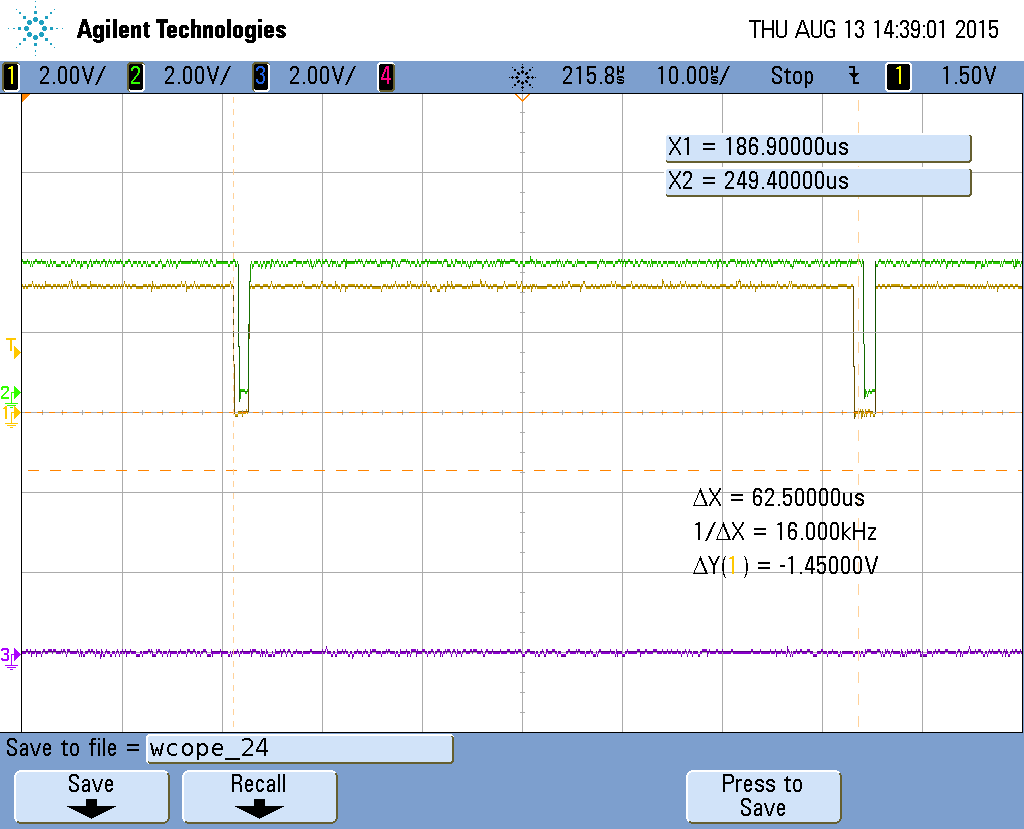
    We found out that sometimes (maybe once in 50 to 100 tries) after power up the four ADS131E08 DRDY outputs are not working completely parallel. Software initialization code gives a Reset command, gives a SDATAC Stop command, sets the data format to 24Bit @ 16 kS/s. After RDATAC command the START input pin is set to HIGH, so that all 4 devices start conversion fully parallel. In error case one of the devices (not always the same) works somewhat distorted – the DRDY signal irregulary goes low one or two clock cycle too early or one or two clock cycle too late. This behaviour keeps to be the same even after issuing a reset command and rerunning the complete initialization sequence. We need to repower the system to come back to normal behavior.

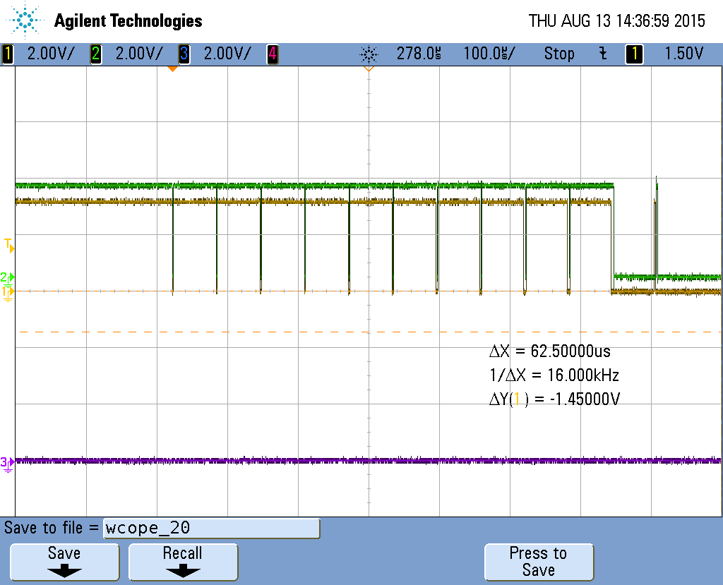
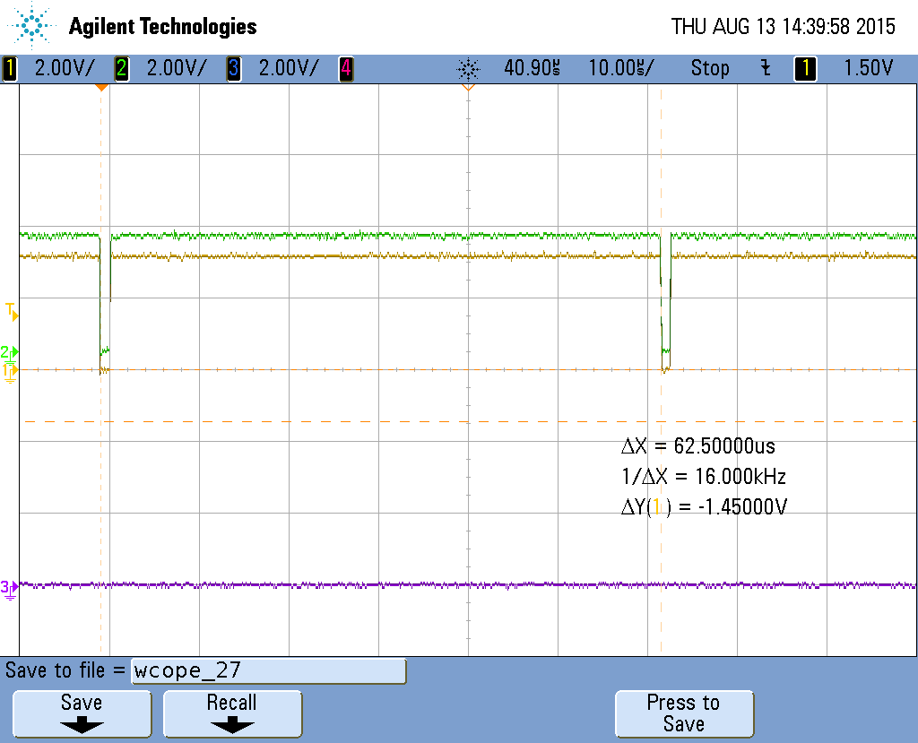
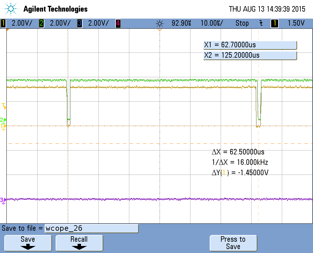
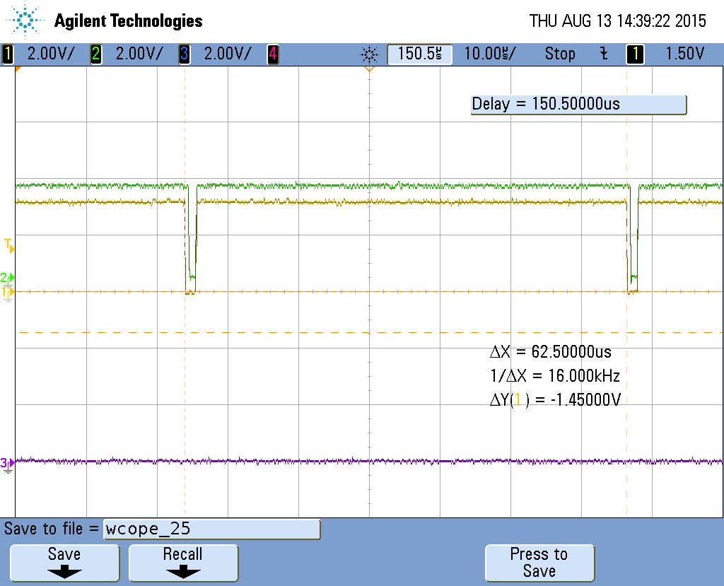
    We have done a lot of experiments regarding decoupling capacitors on the digital and analog supply – with no difference. Clock signal quality of external clock looks perfect (see screen shot).

    It looks somehow that the device with the problem has some curious internal clocking behavior – as if there would be an internal PLL clock generator which is somehow coupled to the external clock and which sometimes does not operate in a stable condition.

    In very rare cases we have also seen situations where one of the devices does not generate a DRDY signal at all (DRDY always HIGH) – all other behavior being the same, no change with Reset command. But mostly we just have the jitter on the DRDY.

    I have investigated already multiple weeks into this issue. Without stable DRDY timing I cannot operate this device, as I need fully parallel sampled data from all channels. I would very much appreciate your help, I am running out of ideas...

    Best regards
    Bernd

    picture 20 overview

    picture 27 first two DRDY pulses look perfect

    picture 26 next DRDY of yellow channel comes one clock cycle too early (500 ns)

    picture 25 next DRDY period: time shift between devices, but same period.

    Picture 24: next DRDY, yellow channel again one clock cycle too early.

    Picture 21: after some more DRDY cycles, time shift between channels is so big that receiving FPGA detects out of phase situation and restarts converters.

  • Hello Bernd -
    OK...I think we have a better understand of your problem now.

    One question...what is that maximum delta that you are seeing between the channels? (or what is your program considering out of sync)

    A couple things to try and may help us understand your configuration and identify the behavior that you are seeing:
    1. (Referencing Figure 46 in the datasheet) The START signal is latched on the rising edge of CLK. You should change START on the falling edge so that all devices sync to exactly the same point/clock.
    2. The RESET signal is latched on the rising edge of CLK. You should try ensuring that RESET is changed on the falling edge for best operation.
    3. Additionally, what does the clock distribution look like for your circuit? Is is possible that there is a delay in the clock signals between the devices?
    4. On the board, how are the devices (and surrounding circuitry) laid out? If you have a section of the board that getting hotter than the others, one of the devices may drift different than the others.
  • Hello Greg,

    thanks for your support.

    We have checked your points, and are convinced that these can not cause our trouble.

    The devices are connected directly to the same clock signal, there is basically no deiay in between.

    We do not give any start or reset signal between the DRDY cycles in parallel working devices. Reset signal is given only as command, start signal is only given once for continuous reading mode. But we see DRDY period lengths to differ for 1 or 2 clock cycles in the parallel working devices with the same clock. We would expect that DRDY timing is fixed to clock cycles under any circumstance. This is definitely not the case in our installation. Sometimes one of the ADC devices shows the different DRDY periods and stops this behaviour only after power down. It is not a stable phase shift between the parallel devices, phase shift changes from one conversion to next conversion. You see the details in the diagrams we sent last time. These diagrams are snapshots of consecutive conversions, showing an increasing time offset between the DRDY signal - although the devices are driven by the same external clock signal. We find this is really strange and must be caused by some very strange behaviour within the device. And we see it only in about 1 of 50 power up cycles.

    By the way, the devices are close together on the PCB and I have measured the same temperature within 1 Centigrade (37.0 to 37.4 °C).


    Do you have any more idea?

    I am really starting to become worried that my device will never work properly...

    Thanks for your support,

    Bernd


  • Hello Bernd -
    A couple more things to consider:
    What does you clock connection look like from the FPGA? Are you using a clock buffer/distribution IC or just trace connecting the FPGA output to each IC? After future discussion, we are concerned that you might be experiencing some noise or spikes on the clock lines that might cause some devices to recognize an extra clock (or similar) that can build up over time to cause the noted behavior.
    What is the duty cycle of your clock? Other than 50/50? If yes, than there could be a similar effect as above.

    Suggestion for testing:
    Do you have the option to use the internal oscillator from one of the chips and send it to the remaining chips in the chain? If so, do you see the same behavior as the external signal?