This thread has been locked.

If you have a related question, please click the "Ask a related question" button in the top right corner. The newly created question will be automatically linked to this question.

ads1230

Other Parts Discussed in Thread: ADS1230

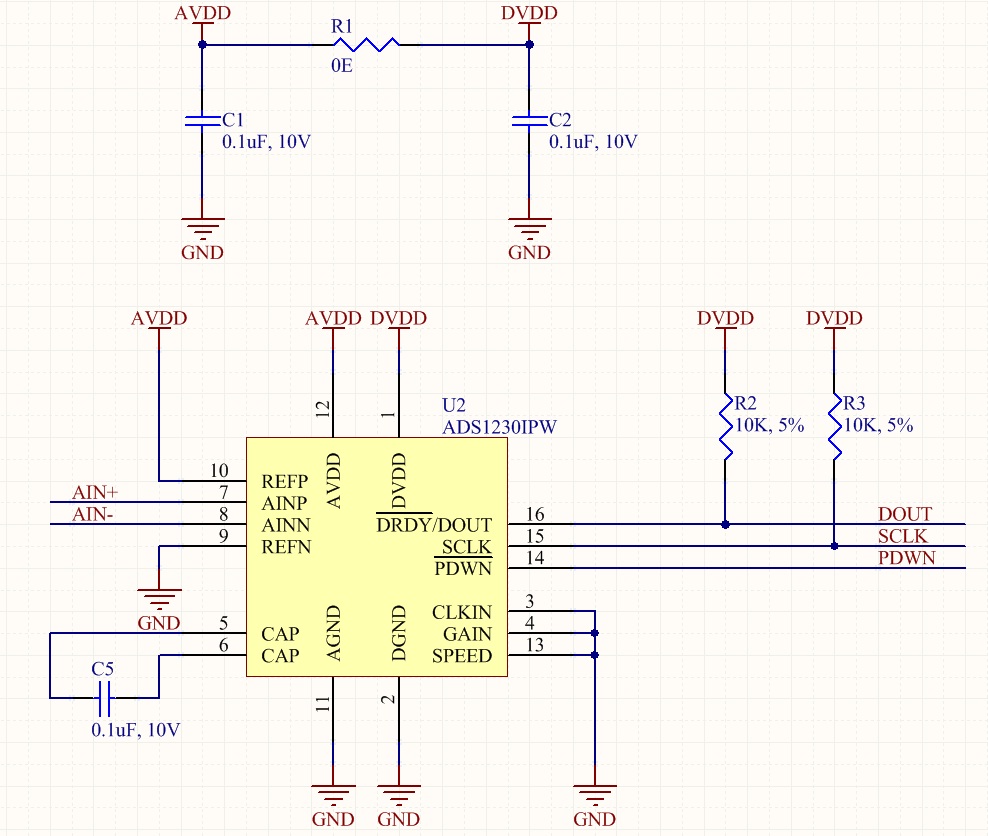
We are facing some problem with the communication to ADS1230 by ATTINY48.


1. As per data sheet CLK pin should be input at ADS1230. But it is giving clock (21 clocks) to Microcontroller.

2. After each time of interval as per data sheet SDA is giving Data ready pulse. But not able to get data as per data sheet CLK sequence.


  • Hi Sheetal,

    The only active digital pin on the ADS1230 is the DRDY/DOUT pin (MOSI).  There is no data in pin (MOSI) connection. 

    It would appear that there may be some confusion as to the mode of communication by the terms used in the questions asked (such as SDA for example).  The ADS1230 is an SPI device and not I2C.  As the ADS1230 does not have a DIN pin, and uses a 2-wire connection I can see how this might be confusing.

    Most microcontrollers require a write to the TX buffer to initiate SCLKs.  Even though there is no connection, you can still initiate the SCLKs in this way, then read the RX buffer after all clocks have been issued.  This is often done in byte increments using the microcontroller SPI peripheral, but you can also write code to bit-bang the GPIO pins instead of using the microcontroller SPI peripheral.  Can you send me the schematic?

    Best regards,

    Bob B

  • Thanks Sheetal/Bob,

    We are able to get data from ADS1230 by using ATTINY48. But there is still some issues. There is some variation in the output of the ADS1230. It is around +-20 to +-30 (Approx +-12.5%). Can you please help me to handle this accurately.

    Regards
    Kushum Rajput
  • Hi Kusham,

    What do you mean by "+/-20 to +/-30"?  Is this codes, weight or some voltage representation.  I have no idea what you are trying to do or what you have connected.  Can you send me a schematic and explain your setup? 

    I will assume that you have some prototype setup.  Any loops of wire will pickup noise.  Poor grounding will also affect your results.

    Best regards,

    Bob B

  • Hi Bob,

    I have connected Load Cell to ADS1230 and reading the conversion data from the ADS1230. There is some fluctuation in the data. Count variation is around +-30 around. Not able to get absolute value from ADS1230.

  • Hi Kushum,

    Do you have any anti-aliasing input filters?  How noisy is your AVDD supply and what is your supply voltage?  Load cell cables are often a source for EMI/RFI pickup.

    From the schematic you are using a gain of 64.  Your best input referred noise is when you use the highest gain setting.  The noise tables on page 6 of the datasheet show you the best possible noise performance of the ADS1230.  You will never achieve a totally stable noise free resolution out to 20 bits.  Also remember that any noise on the reference will be reflected in the ADC measurement.

    To analyze the source of the noise, it is best to use a shorted input at the ADS1230 biased to the correct common-mode.  The easiest way to do this is to create a voltage divider of equal resistances between AVDD and AGND.  Connect the shorted inputs to the voltage divider at mid-AVDD supply.  This is the best the system can do relative to noise.  You should be able to duplicate the values seen in the datasheet noise tables.  If you cannot, then the likely sources are supply/reference noise or layout issues.

    If you receive good noise results for the shorted input case, then you will need to eliminate noise on the input path.

    Best regards,

    Bob B

  • Hi Bob,

    Thanks for the suggestions. We will try to do some experiments on this. Will update the results to you. attaching the load cell connectivity circuitry also.

    Regards

    Kushum Rajput