Hi, I have some problems with using ADS62P20EVM in CMOS mode, and I was wondering if anyone can provide some suggestions.
I configured the ADC to work at CMOS mode by setting JP14. The input clock is in burst mode- multiple cycles of 100MHz square wave with VH=1.5V and VL = 0V.
the outputs of ADC are routed to a FPGA evaluation board (Xilinx ML605) by TI's FMC-ADC-ADAPTER. IOSTANDARD of the FPGA is configured to be LVCMOS. Vcc of the bank is 2.5V. According to the datasheet, VIH is 65% of Vcc, so 1.8V output voltage should be enough.
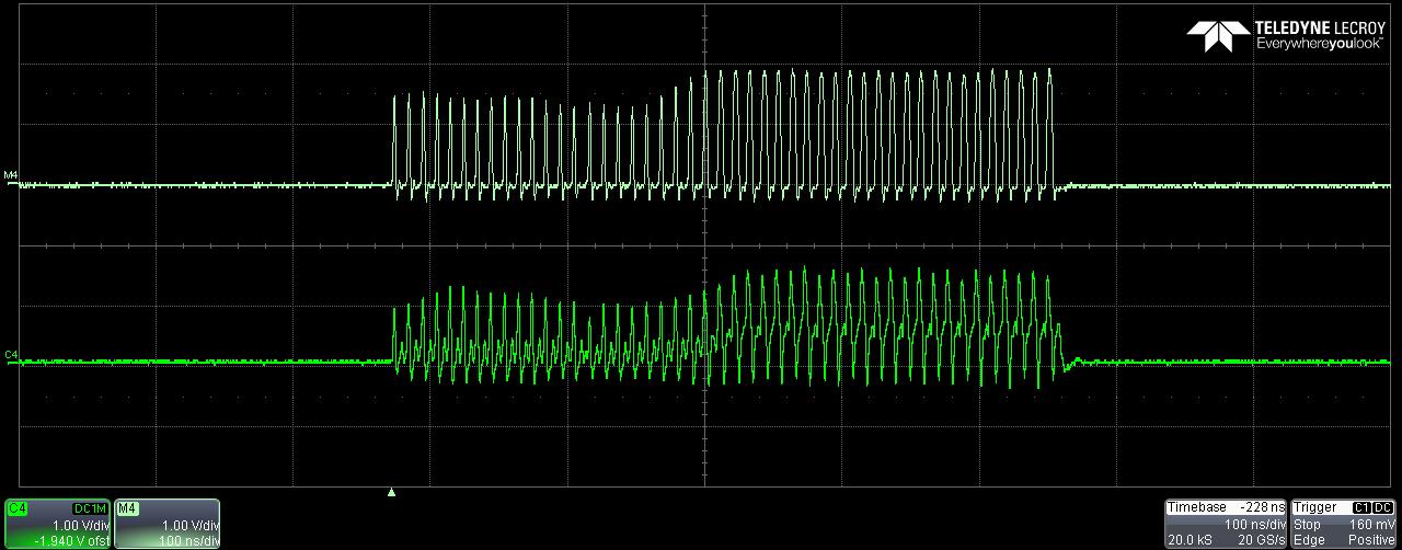
But when FPGA board is connected, the output clock of the ADC becomes strange. In the figure below, the white line is the output clock of ADC without FPGA board, and the green line is with FPGA board. It seems there is impedance mismatch, which I do not understand. Can anyone point out what I have done wrong? Thanks.
Lingmei