This thread has been locked.

If you have a related question, please click the "Ask a related question" button in the top right corner. The newly created question will be automatically linked to this question.

ADS1248 anti-alias circuitry, and sequencing multiple channels

Other Parts Discussed in Thread: ADS1248

Hi folks:

I am designing an ADS1248 system, and have a good handle on the pga setting, CM range implications, and spi interface, but I have few questions:

Regarding anti-alias circuitry, I have looked through the forum and found a related post where Joseph Wu replied "for anti-aliasing, you want to be basically half the modulator rate."  This adc will be modulated at 512 KHz.  Though I will use a much lower bandlimit in my  design, do I only need to bandlimit my inputs to less that 256 KHz to prevent any aliasing?

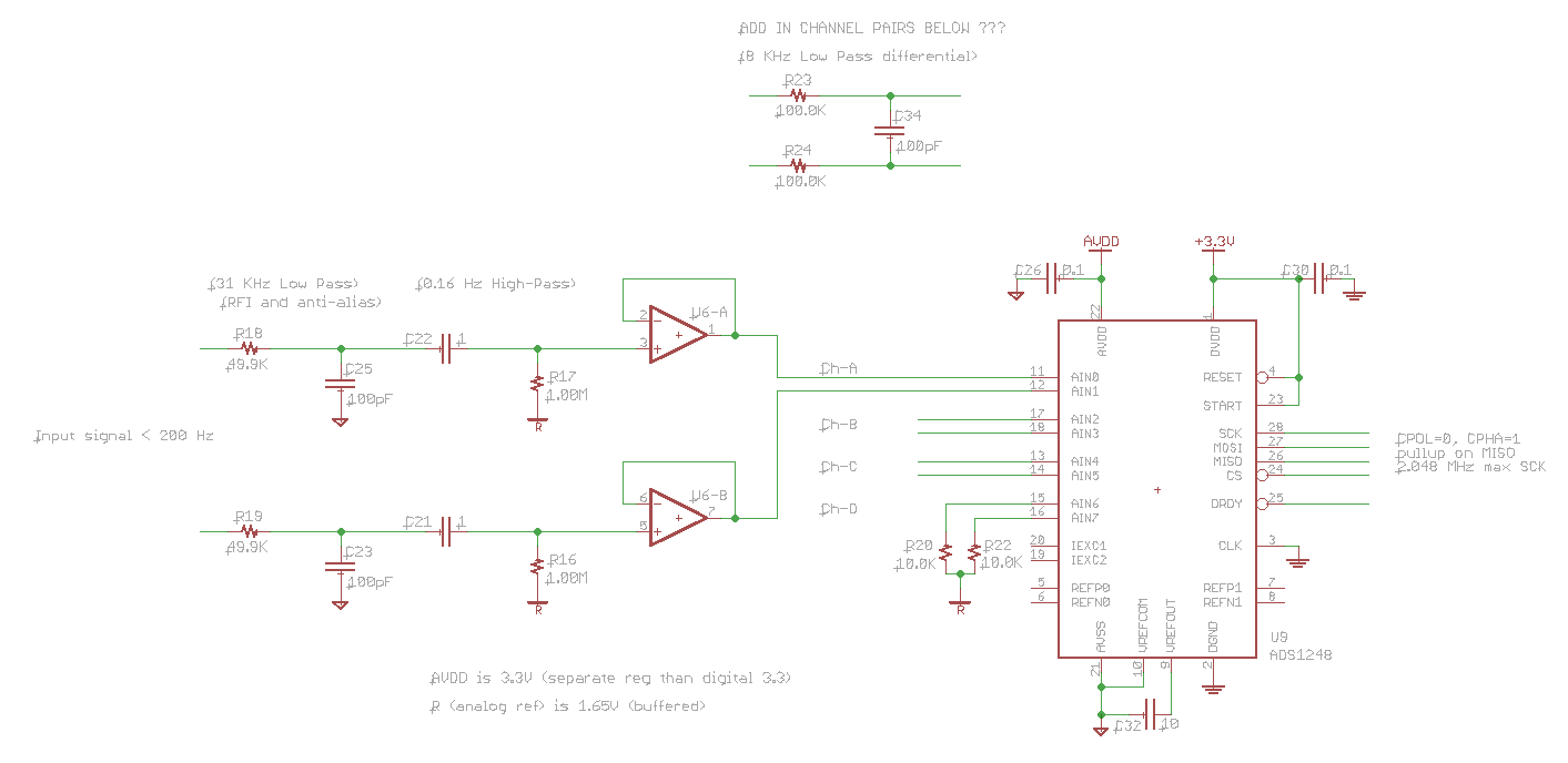
My tentative circuit is below.  I have three differential input signals with a band of interest below 200 Hz (input circuit is only shown for one channel).  Each line of each channel must be independent (no differential filtering allowed on these inputs) and has a separate input filter (0.16 Hz to 31 KHz) and a buffer.  In the EVM schematic I see a differential filter before the adc inputs.  Is there any reason I should add an additional differential filter between my buffers and the ADC, as shown below?


I also see 10uF bypass caps on the EVM, but no mention in the datasheet on bypassing -- is 10 uF needed or is 0.1 uF enough?

One last question:  I plan to run at 2000 sps, sequencing each channel (the 4th chan is a spare), which should give an effective 500 sps rate for each channel.  Does this then mean my -3dB bandwidth of each channel is about 346 Hz (interpolating the 320- and 640-sps datasheet specs).

thanks,

Gil


  • Gil,


    For anti-aliasing, you need to be at half of the modulator rate. At 2kSPS for the data rate, the modulator runs at 512kHz, so you are correct that the filtering need to be at 256kHz.

    I'm not sure about your input schematic. At this point you have the inputs buffered but nothing establishes the input-common mode voltage of the input signal. Part of the problem is the high-pass filtering that you have. If you need something similar to this you could use a fully differential amplifier with an output common-mode setting. Depending on what you are measuring, I would have used simple passive filtering. Why is no differential filtering allowed?

    I personally think that 10uF is a bit high for bypass caps. I realize that's what's on the EVM, but I think that 0.1uF is just fine.

    If you're running at 2kSPS, look at Figure 64 (which I think you may already be aware of). It will show you the frequency response of the ADC based on the digital filter used after the modulator to give data. It already has a -3dB bandwith of about 1.5kHz. If you are taking every fourth sample, you would effectively be dividing the bandwidth for 2kSPS by four (it's more complicated than that, but its a good ball park number). Your estimate of 346Hz would have been pretty close anyway.

    One thing to note about running at 2kSPS is that there are some specific requirements about the SPI communications for proper operation. If you look at the datasheet on page 34, there is a section on Single-Cycle Settling that you should read through.


    Joseph Wu
  • Gil,


    One other point that I forgot to make was that if you were to do passive input filtering (with series resistance and a capacitance), I would use lower input resistances.

    Generally 1kOhm or less is fine. In some cases, I've seen 10kOhms, but the series resistance reacting with the input bias currents can become a problem (there may be linearity issues with large resistances because the input sampling requires extra settling time).


    Joseph Wu
  • Hi Joseph:

    Thanks for the input. It is good to be sure about the anti-alias freq, bypassing, and a ballpark on the bandwidth of 2000sps/4 sampling.

    It is interesting that the SPI rate is rather limited to 1.92 to 2.048 MHz (and other misc requirements), but that is easy enough to control.

    Regarding my inputs: I cannot do differential filtering since the inputs are not all independent (specifically, one input is the negative input to two channels). I have a low pass RC (to analog ground) at 31 KHz -- this provides simple RFI filtering, plus bandlimits for anti-alias needs as well). Next I have a high pass RC at 0.16 Hz that feeds the buffer -- this resistor refers to 1/2 supply (a low-impedance 1.65V) so the buffer is indeed referred to the center of the 3.3V analog supply. Am I missing something?

    On the possible differential filter between the buffers and adc: yes, the 100K values are kinda high, but the Zin of the adc is also way-high, However, you bring out an interesting point I had not considered about the bias currents causing some more error with higher resistors. I could get the same rolloff with 100-ohm/0.1uF or something in between.

    Is there an advantage to a true differential filter here though?

    thx, gil
  • Gil,


    I agree with the RC low pass to ground acts as an RFI filter, however I don't think the high pass works. What ends up happening in steady state is R17 and R16 will pull the buffer input to ground.

    The differential cap is really there for anti-aliasing. In your case, you really have some filtering that works for common-mode filtering, so at some point, there may be some common-mode signal that can be seen as differential if the filters aren't matched. However, if the frequency content drops off fast, it may not be that big of a deal.

    As for the 100k resistors, yes the input bias currents add errors, but you may introduce a larger non-linearity error with large series resitances. Since the input is based on sampling a capacitor into the modulator, it needs to be able to sample and settle within the modclk time. With a large series resistance, this may disrupt the sampling and may cause a non-linearity error near an input of 0V.


    Joseph Wu
  • 'nuther quick note:

    I need at least 40-ish K-ohm series input resistance on the inputs, so that starts the passive net design. I can't lower these resistors. I can do whatever I want resistor-wise between the buffers and the adc, but not on the inputs. I also need the low-output-impedance of the buffers since they feed other analog circuitry, not just the adc.

    I wish to use the differential adc inputs in place of expensive and bulky instrumentation amps (which would then still need a single-ended adc, or a diff adc simply referred to vdd/2). I have done this quite effectively on a previous product (now in production) with a higher-end '1294. This is a different application, but I want to do the same thing: differential inputs are filtered and fed to a differential adc -- no instrumentation amp needed. Powerline and other CM effectively removed in the process. I am just not certain whether I am filtering (and bandlimiting) correctly.

    Any advice appreciated.

    thx, gil
  • Ahh, I was typing before I got your response. Yes, it make lots of sense to keep the resistors before the adc low, and it sounds like an actual differential filter there makes sense as well. Also a good point about filters not being matched and CM becoming DM -- very good point indeed.

    But just to point out: the R16/R17 do not pull the buffers to ground, as they return to 1.65V (1/2 of AVDD=3.3). The schematic symbol is different that the AGND symbol, but is a a bit subtle.

    thanks for your help. gil