This thread has been locked.

If you have a related question, please click the "Ask a related question" button in the top right corner. The newly created question will be automatically linked to this question.

ADSXX53 TINA - Undersampling

Other Parts Discussed in Thread: ADS8353

Hi,

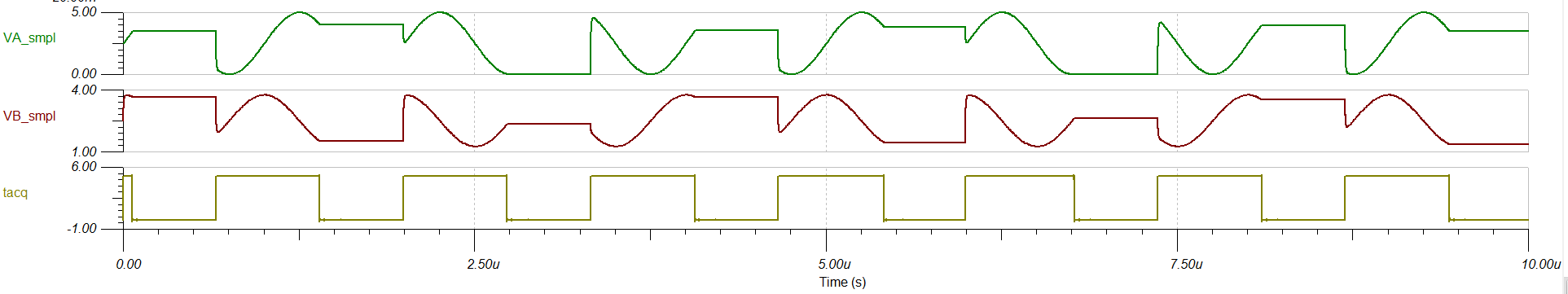
I am using the ADSXX53 TINA model to obtain simultaneously sampled signals, my application requires undersampling with a much lower rate than the input signal.  When I input a high frequency signal relative to the sampling rate part of the input signal appears at the output of the ADC which ideally should not happen, my understanding of the operation of an ADC is that it holds the current value until the next sampling clock so the signal should appear quantized. Is it something with the model that makes the input equals to the output while the acquire signal is high ? Is there a way  in TINA to just get the sampled values ?

  • Zaid,
    The model was done by the device's product line. I am moving your inquiry to their E2E forum. One of their experts will be able to help you.
    John
  • Zaid,

    The ADSxx53 TINA Spice model allows to perform a transient simulation to observe the settling of the voltage of the internal sample-and-hold capacitor at the end of the sampling period.  These TINA Spice SAR models simulate the loading characteristics of the ADC input pins so that users can test the amplifier driver circuit for settling accuracy.  

    The model does not return automatically the quantized discrete sampled voltages; however, it allows the user to confirm the voltage in the sample-and-hold at the end of the sampling period when the sampling of the signal occurs.  In other words, by performing a transient simulation and plotting the Vx_smpl signal, the user can see the the voltage that is sampled at the falling edge of the tacq signal.  TINA allows you to zoom in the transient plot and by using the cursors, the user can determine accurately the voltage in the sampling capacitor at the sampling instant when the falling edge of tacq occurs. 

    Please find attached a blog discussing this topic with an example.  The example provided in the blog is for a different model but the same principle applies.

    Please let me know if you have questions.

    Best Regards,

    Luis

  • Thank you Luis for your prompt reply. I understand the purpose of the model, just one quick question, the timing diagrams in the data sheets do not seem to match the model's clock, I just want to know how to tweak the sampling rate, changing the overall clock period without altering the pulse width seemed to work on the model, otherwise it behaves unexpectedly. Is this the way to do it, just increase the clock period and keep the pulse width the same, the model automatically adjusts the acquire time ?

  • Hi Zing,

    The model is based on the ADS8353 (16-Bit) version which only supports the 32-CLK digital interface mode.   The 14B and12B versions support both 32-CLK mode or 16-CLK mode of operation.  When using the 32-CLK mode, the conversion time is constant.  The falling edge of CS triggers the conversion, where the acquisition phase (or sampling phase) ends at the falling edge of CS; and the conversion time starts. The device returns to acquisition mode immediately after a fixed conversion delay (~630ns typ).  By adjusting the timing between CS falling edges, the user can adjust the data rate.  Attached is a modified file where the device is set up for 100 KSPS.  To adjust the data rate, I extended the interval in time between CS falling edges.

    Please let me know which resolution (16B, 14B, 12B), interface mode (32 CLK or 16 CLK), and data rate is required in the application; and I can look into providing the modified file.

    Thanks and Regards,

    Luis

    ADSXX53_sampling100kHz_modified.TSC

  • Thanks Luis, for the explanation and the modified file. I see now how I can successfully alter the sampling rate. I am considering buying the evaluation kit of the ADC, but I am wondering if I can implement a random or non-uniform sampling scheme on it. I went through the data sheet to see if there is any setting in the registers that might help me to do that, but I could not find any. The only way I am thinking of, is to change the clock period after each conversion in a certain time window. I saw on the software of the evaluation kit the sampling rate can be altered, but I doubt I can automate it to achieve random sampling in a narrow time window, can you please advise regarding this manner. What would be the best way to do it using resources available from TI.

  • Hi Zaid,

    The ADSxx53EVM-PDK demo kit provides options for a couple of data rates, however, the settings are manually changed through the GUI.  In order to change the sampling rates in a automated fashion in a narrow time window, you will need to develop software to support this application.  You could interface the existing hardware through the SDOA/B, SDI, SCLK, CS lines to a host microcontroller, DSP or digital I/O card with a serial port supporting the required SCLK frequency . The data rate is controlled by the timing period between CS falling edges.

    Best Regards,

    Luis