This thread has been locked.

If you have a related question, please click the "Ask a related question" button in the top right corner. The newly created question will be automatically linked to this question.

ADS1248 GAIN PROBLEM

Other Parts Discussed in Thread: ADS1248

Hi 

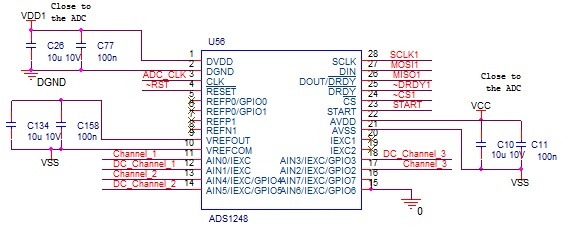
I having problem with series of ADS1248 that used with same code 

some works and some has greater gain

the code is using accurate external clock to for timing 900Hz in 2000 samples per second 

the pseodo code is as follow

in the start of the code i Initializing 

RESETn=0
wait 500us
RESETn=1
wait 50ms
START=1
writeSPI(WREG+MUX0)
writeSPI(3)
writeSPI(P_AIN0+N_AIN6) or writeSPI(P_AIN4+N_AIN6) or writeSPI(P_AIN2+N_AIN6) // change sequentially
writeSPI(0)
writeSPI(0x30)
writeSPI(0x0F) //rate: 2000sps gain: 1

then i reading using RREG to verify writing is good

timer at 900Hz trigger interrupt that:

Start=1
wait 1mSec
CSn=0
writeSPI(WREG+MUX0)
writeSPI(3)
writeSPI(P_AIN0+N_AIN6) or writeSPI(P_AIN4+N_AIN6) or writeSPI(P_AIN2+N_AIN6) // change sequentially
writeSPI(0)
writeSPI(0x30)
writeSPI(0x0F) //rate: 2000sps gain: 1
Start=0
CSn=1

wait for DRDYn to go down

CSn=0
writeSPI(RDATA)
readSPI(result[][2])
readSPI(result[][1])
readSPI(result[][0])
CSn=1

I tried many configurations an my final conclusion is that either you have defected series
(working DXXX, not working CXXX)
both bought from digikey
or I am doing something wrong 

please help

  • Shaii,


    First, I have a few questions about gain issue. All of these questions are important to see where this problem comes from so read through them and see you can get back these answers.

    How much is your gain off from ideal? Is it off by more than 1%? or is it extremely large (like 25%)? Does this happen with all units or is it isolated to just one or just a few?

    Does the gain error change when the data rate changes? Can you slow down your setup, and try using several of the other data rates? Can you report the OFC register contents and the FSC contents? Do you have a logic analyzer to make ensure that the communications that you have coming out of the device is correct?

    What are you measuring? Are you using the internal reference or an external reference? If you are able to share a schematic (or a portion of the schematic) it might help. Also, are you measuring back the input and the reference voltages to make sure the ADC isn't working properly? You may need a precision multimeter to make this measurement.

    I may have other follow-up questions later, but I'll start with these. Hopefully we can get a solution soon.


    Joseph Wu
  • Shaii,


    Also, I need to know more about your configuration. What gain are you in? What is your input voltage and what is your input common mode voltage?

    One common gain problem is that the input common mode voltage has a specific range with the ADC. It's listed in the Electrical Characteristics table, but described more in the Low-Noise PGA section on page 26 of the datasheet.


    Joseph Wu
  • Hi Joseph

    Thanks for the quick response

    1. the gain is much higher then 4  (cant know for sure, i can check)

    2. the new units that i bought in 3 batches (all of them from series cxxx) are bad

    3. the data rate is good the timing is good (DRDYn goes down on time) . cant slow down

    4. I have logic i verified the signals looks good.

    5. Tuesday i will report The OFC and FSC register content.

    6. i am measuring voltage from output of Operational amplifier (-1.5 to 1.5)

    7. I am using internal reference.

    8. i used DMM to verify the voltage reference voltage and the input voltage.

    9. i also in several cases replaced the ADC with one from different series and the circuit started working.

    10.schematic:

    VSS=-2.5

    VCC=2.5

    DGND=0

    VDD1=3

  • Shaii,


    When you get the bad gain error, how much is it?

    What is the input voltage that you are reading and what is the output data (output code, not the converted voltage).


    Joseph Wu
  • Hi Joseph

    Those are the registers reading in perfectly working ADC (DHY0 series)

    0x06

    MUX0

    0x00

    VBIAS

    0x30

    MUX1

    0x0F

    SYS0

    0x00

    OFC0

    0x00

    OFC1

    0x00

    OFC2

    0x80

    FSC0

    0x0A

    FSC1

    0x40

    FSC2

    0x90

    IDAC0

    0xFF

    IDAC1

    0x00

    GPIOCFG

    0x00

    GPIODIR

    0x00

    GPIODAT


    Those are the registers reading in Non working ADC (CSDL series)

    0x06

    MUX0

    0x00

    VBIAS

    0x30

    MUX1

    0x0F

    SYS0

    0x00

    OFC0

    0x00

    OFC1

    0x00

    OFC2

    0x00

    FSC0

    0x08

    FSC1

    0x40

    FSC2

    0x90

    IDAC0

    0xFF

    IDAC1

    0x00

    GPIOCFG

    0x00

    GPIODIR

    0x00

    GPIODAT


  • GAIN=1
    AVDD=2.5
    AVSS=-2.5
    VCM max = +/-0.75
    -2.5+0.1+1.5/2 <+/-0.75 < 2.5-0.1-1.5/2 it on the right range
  • Hi Josef

    I have new input

    when i shorting both P and N to GND

    this is what i get (normailized to volt +/- 2.048) 

    when i change to different series its showing the noise floor as expected

    Shai

  • Shai,


    I've never seen anything quite like this where the problem is lot dependent, so I have a few more questions.

    I was going to ask what the gain error is when you have a bad measurement, but it looks like the error is mostly a random output. The graph that you provided looks a little like a digital communication error. The reason I say this is that the resulting data is a structured. It's almost like trying to read a full scale data, but the input sometimes reads full-scale, sometimes reads half-scale, sometimes reads quarter-scale etc. This looks as if the data is bit-shifting through. With the inputs at GND (which is outside the common mode input range with a single supply), you should still read something near 0. Do you have the raw data for this plot? I'd really prefer to see the digital output data instead of the converted data.

    If you do get devices that perform with real output data, what is the gain error? I'd like to know if this is really isolated to this lot and if there are ones that give you some real data.

    Also, I'd like you to confirm some of the digital timing. First check that the SCLK idles low and that the data is read in on the falling edge. This can cause some data that looks like it's bitshifted. I'd also like you to check the SCLK speed and the timing with relation to /CS. I could see that a timing error might be lot dependent, so I want to check this as well.

    The only other things that might be in error if there is some sort of violation of common-mode input range (even momentarily) that might be seen in the next reading. If the input is over-ranging the PGA, then the input might have a long recovery. If the inputs are changed and moving from channel to channel or a reference is turned on and off or switched, there might be some settling time involved. For all of the overloads, the recovery time might be lot dependent (I find this a bit unlikely, but I still want to check).

    Have you ever changed the data rate or extended the length of timing for a data read to see if it helps?

    How many units of the C series do you have?

    Finally, may I contact you through the email address that you supplied through the E2E signup? I'd like to get some direct communication. However, I would like you to consider all of these questions that I've written into the post and get me some specific answers. I'll need more details to even guess what the problem is.


    Joseph Wu
  • Shai,


    I also forgot to ask about your digital communication. Do you issue an SDATAC and just use RDATA for subsequent reads, or do you use the /DRDY as an interrupt to read data? If you use the latter /DRDY method with RDATAC (which is default), make sure you clock out the data before the next /DRDY comes along or you may get corrupted data because the DOUT has been updated with a new reading.

    It might help to get a oscilloscope shot of the communications capturing the SCLK, DIN, /CS, and DOUT. It might also help to have a couple of examples of the /DRDY timing with the reading of the data. A logic analyzer would certainly help capture all of these lines and get the timing.


    Joseph Wu
  • First i thought its gain error but  its appear to be some kind of noise outside the scale of the input.
    its not communication problem because i checked it with oscilloscope (In MSP430 UCCKPL=0 UCCKPH=0)
    i agree that it look structured so i thought maybe i didnt give enough time to settle and it didn't work
    I have degenerated the problem further more
    i took new card with machine soldered component with CSDN series device
    changed the parameters to 1000 samples per second
    START constantly up
    both p and N tied to GND
    OFFSET and GAIN register verified fine
    I verified the voltages applied are good
    and here I get on this device constant 7FFFFF
    I changed it to the old serie and it works fine.

    all the devices from CSDN and CSDL doesnt work good (i have about 30 units)
    the problem is that the project is before mass production and this is very big problem for us


    my guess is that something causing the sigma delta modulator to fail convergence.
    In the second after power up, i am getting near zero readings and after few seconds it starting the problematic behavior
    but still the thing that odd is that with old series it working and somehow something is different 

    you are welcome to contact me in email.

  • I just use RDATA after DRDY interrupt
    I am clocking out the data immediately after /DRDY goes down
    I am using oscilloscope to see the data and its matched
    again, i think those units are faulty but if they are why you didnt notice it before?

    Shai
  • Shai,


    I'll go ahead and contact you directly through email. I don't know what the problem is, and we've never seen anything like quite like this. I have seen delta-sigma modulators become unstable, but it's usually because of some large input signal of high frequency that is out of band. In those cases though the output would stay near 0 and then give bursts of noise. This still looks different to me.

    Here's what I think we'll need. I like to see a complete schematic and a bit of an explanation of what you are measuring. It should include the full signal path and whatever you are measuring. I see that you cycle through 3 of the inputs, do you use the IEXC to source current through a RTD or some other bridge type measurement?

    You've taken some oscilloscope photos of the data exchange, I'd like to see them. I'd definitely like to see all of the digital lines plotted. This would include DIN, DOUT, SCLK DRDY if you can only get 4 channels. Capture /CS on another plot with the others minus /DRDY.

    I saw the graph of the data when it's bad. I'd also like the data when it is good. Also, I'd like an excel file of an example of good and bad data in the output code in hex, not the converted data in Volts.

    Are you using the internal oscillator or an external clock? What is your SCLK speed?

    Finally, I'd like the full marking on the device. This way, I can have the history of the lot tracked. In the meantime, I'll look at how we can get a few of these units to look at and how we initiate a customer return.

    Again, I'll contact you directly and we'll take this offline.


    Joseph Wu
  • Shai,


    Did you receive my email? I wanted to make sure that you were able to contact me.


    Joseph Wu
  • The problem seen with the device is the voltage required for operation with bipolar supplies. With a low bipolar supply, the problem is in the communications between the analog and digital sections internal to the ADS1248. There are digital circuits within the analog section that still need to communicate with the digital section. Since they operate on different supplies, there are level shifters between the two sections that allow for communications. I believe that this is the problem with the data. There may be some problem with the clocking structure between the analog and digital section, or a bad modulator output. Regardless, it comes up with bad data at the output.

    For the level shifter between the analog and digital sections internal to the ADS1248, the critical parameter is the voltage step from the analog supply to the digital ground. According to simulations, there is a minimum of 1.93V required from AVDD to DGND. This accounts for variations in process and temperature (problems at cold). There may be some dependence on data rate because the modulator runs a different rates and there may be a settling time component to this problem. However for the time being, 1.93V minimum from AVDD to DGND should be the important specification to watch.

    Shai,

    If you have any more questions or if you continue to have problems with using this device, please feel free to contact me through email.


    Joseph Wu