This thread has been locked.

If you have a related question, please click the "Ask a related question" button in the top right corner. The newly created question will be automatically linked to this question.

Is there an error in lane numbers on TSW38J84EVM and DAC3XJ8XEVM boards?

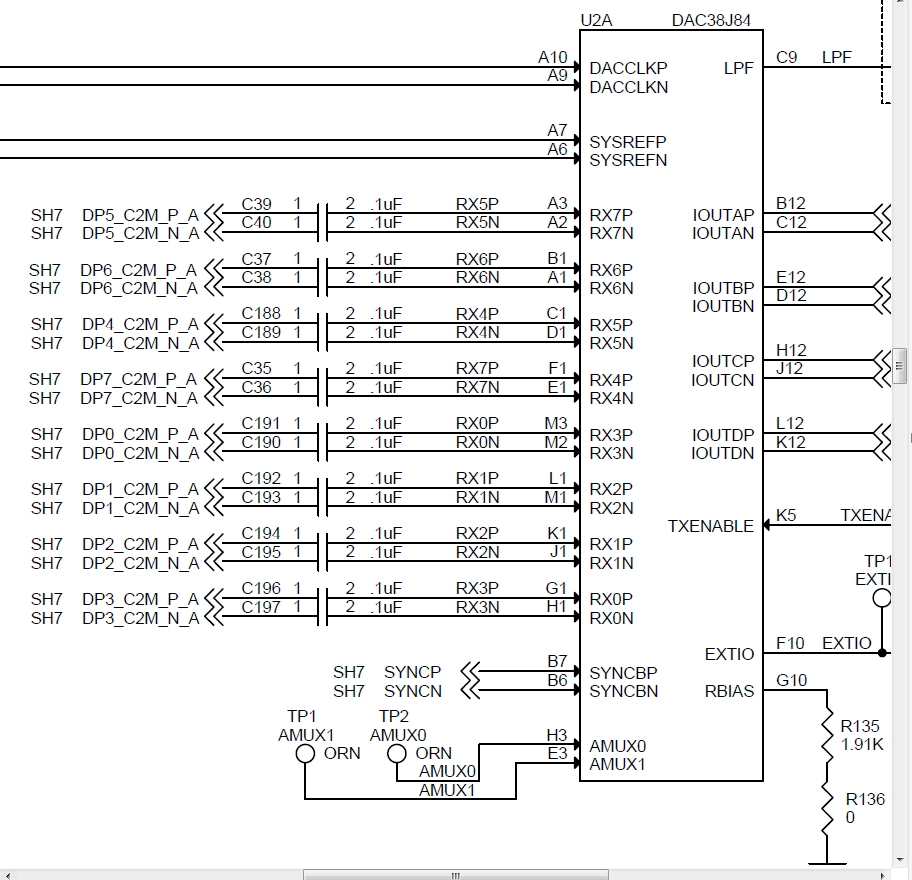
In the schematic package for both the TSW38J84 EVM and for the DAC3Xj8X EVM, there seems to be something strange about the signal labelling on the page marked "DAC" (for both EVMs). This appears to be the same schematic page copied for both EVMs. The 8 SERDES lines coming in to the DAC on the left seem to not go to the corresponding inputs on the DAC. For instance, the lane marked DP3_C2M goes to RX0. I would have expected it to go to RX3. In fact, DP6_C2M does go to RX6. I would like to know if this is important for a new design, or if it is some sort of typo?

  • Gordon,

    The serialized input lanes routing is based on the TSW14J56 FPGA EVM. Due to the layout from the FPGA EVM to the DAC EVM via the FMC connector, we have to use different lane numbers from the FPGA to the DAC SERDES RX port. You may refer to the EVM layout files on the TI web. We simply rearranged the serialized input data on the TSW14J56 side (via HSDC PRO software) accordingly to ensure the FPGA/DAC SERDES ports are matched.

    -Kang