This thread has been locked.

If you have a related question, please click the "Ask a related question" button in the top right corner. The newly created question will be automatically linked to this question.

TSW1400EVM Firmware Source for AFE5851EVM (16 channels ADC)

Other Parts Discussed in Thread: AFE5851EVM, AFE5851, AFE5808

Hello, 

My team want to use AFE5851EVM and TSW1400EVM to implement our system.

We have tried to combine these two evaluation board,
and use the software on the TI website to capture the data. (AFE5851 and HSDC Pro)
And also have solved some problems on it.

Now we want to add some functions into the firmware for FPGA.

So we have to get the verilog source code for the AFE5851EVM.

Because we tried some other ADC boards to capture data before. (AFE5808、5809)

I have got a version of verilog source code.(like below picture)

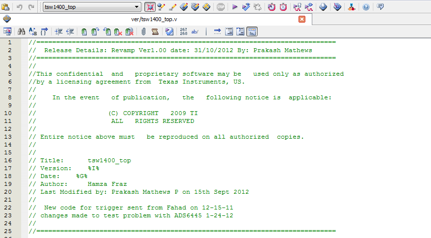
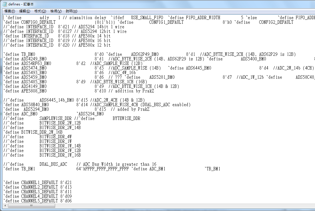
But it seems not work for AFE5851.

My questions are:

  • Does the version verilog source code work for AFE5851EVM?

If it can work for AFE5851EVM, then what settings do I changes?

If it can not work for AFE5851EVM, where can I get the correct version source code? 

Kind regards,

Jhin Ci

My email:

JhinCiHong19901008HY@gmail.com

  • Jhin,

    I'm assigning your post to the appropriate apps engineer. He should respond soon.
  • Hi Amy,

    Thank you for your assigning.

    It have been a few days since I posted this question.

    If I can get the right source code or correct setting quickly, I would very appreciate.

    And I want to explain more about what our team would implement in FPGA.

    In FPGA, we want to implement several parts.

    1. ADC data capture  (into DDR2)

    2. PC read DDR2 from FPGA

    3. MUX controller    (control digital output)

    4. Control DAC chip   (also control digital output)

    5. Others ...

      More detail :

        Part 3 and Part 4 is easy to design.

        Part 1 and Part 2 are the main parts that we might ask you for help.

        We would contain verilog source code you have designed, just modify some for our purpose.

    But first,

    We have to use verilog source code replaced the HSDC Pro firmware.

    Make sure the source code can work.

    And then we can modify it.

    Kind regards,

    JhinCi

  • Jhin,

    This code does work with the AFE5851, however this code is generic to the ADC and simply streams bits, not samples, to the memory and dll.  We configure the sample structure using a dll that talks to the configuration registers in "Dumpmem Bridge" (FIFO).  I will send another version of the code that might be more specific to the actual device.  I will send this to your email. However,  in general we can't support this code, it is just a reference.

    Thanks,

    Chuck

  • Hi Chuck,

    Thanks for your reply.

    And I am glad to see you again on the E2E web.

    I understand that this code is generic to the ADC.
    And I have this version mentioned in the post and another version named ver1.11.
    So are these two codes work with AFE5851EVM ?

    And most I want to know in these codes is that where do I change some settings according to AFE5851EVM.
    So when I convert source code from verilog to " .rbf " file with Quartus II
    and use HSDC Pro " download firmware " to TSW1400EVM, I can work perfectly as I use HSDC Pro with AFE5851_12X firmware.

    Because the AFE5851EVM is 16 channels input which is different to other ADC.
    There must be some setting have to change in defined files or other place.

    ==========================================================================================

    In addition,

    I have study source code a few days.
    And I want to explain what I understand.

    If there is any wrong in the explanation, please let me know.


       In this system ADC , FPGA and Computer.  (AFE5851EVM, TSW1400EVM, PC)


       ADC part is simple.
       When PC connects to ADC with USB port and sends parameters to the ADC, it just continuously transfer data and clock to FPGA.

       Between FPGA and PC.
       After these two connect perfectly, PC would send command to FPGA using USB port like capture command. (spi_xxx in FPGA as input and output.)
       And FPGA read this command(dumpmem_config_inst) and do correct things.
       
       Main function in this source code is that
       FPGA will read ADC data from LVDS and convert to channels data (adcif_inst, din and dout)
       and then convert channels data to memory data(dumpmem_bridge_inst,din_fifo and dout_fifo),
       then put into DDR2 RAM.
       After all is done, FPGA takes data from memory(dumpmem_inst) and transfer this data to PC.

       Is there any wrong in my understanding ?

    Kind regards,
    JhinCi

             p.s. It is my first time to use TI evaluation board to implement a system.

               If there is any problem which can't talk about on the E2E web or you can't support or offer something, you can just let me know.

               Or we can talk with email.