This thread has been locked.

If you have a related question, please click the "Ask a related question" button in the top right corner. The newly created question will be automatically linked to this question.

ADS1246 RDATAC consistent reading issue, spike every couple of minutes.

Other Parts Discussed in Thread: ADS1246, REF3125

Hi,

I having an issue with continuous ADC reading. Spike of data every couple of minutes, in both direction, positive and negative deviation from the real level of input signal. There is the same spike if inpits are open. I am using default setting with one adjustment - speed from 200ms to  25ms. Command is: 0x43, 0x00, 0x03. I can prove that with the scope on pin DRDY. I am using ADS1246 to read analog inputs (4..20mA with 124ohm conversion resistor). My source is battery pack with pot. Please enclosed: Reference voltage 2.5VDC, ADC circuit, scope images:initialization, rea    dng.

Thank you in advance for help.

Regards,

Dian   
  • Dian,


    First, can you let me know which each trace is for the scope shots? I'm guessing that yellow is /CS, and blue is SCLK, I assume that DOUT is either purple or blue. It would be nice to capture /DRDY as well (if you have to remove one of the lines, I'd say that DIN is the least useful).

    Are you using /DRDY or DOUT/DRDY as an interrupt to read the data? This is important because new data comes out on DOUT for each read of the ADC. As an example you get the DRDY pulse, and then start the read. If you don't complete the read by the time the next ADC data is ready, the DOUT simply updates the data with new data. What you read as data is a combination of the first few bits of the first data and concludes with the first few bits of the new data. This of course would be wrong.

    My guess would that you have an error where the read is delayed so you have this type of an error.

    Regardless, can you take a long stream of data (with a couple of and put it in an excel file? I'd like the raw data from the ADC (not converted to voltage or other value). I'd be ok with the hex data output. Just make sure you mention what the input voltage is at the time (assuming the 2.5V reference).

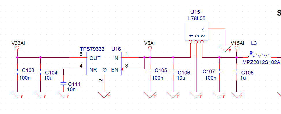
    Looking at the schematic, I don't see too much that's problematic. Generally I won't use any inductors near the ADC. Since there's a large amount of digital currents, even in the analog section, there might be voltage spikes from the Ldi/dt.

    I would also use a lower noise reference than the REF3125. The REF5025 would be a good choice. Since the ADC measurement is a comparison between the input and the reference, the reference noise is a contributor of the noise you see in the ADC.


    Joseph Wu
  • Thank you Joseph for fast respond, I will try the suggestions later today.
    Regards,
    Dian
  • Dian,


    One other thing that might be an issue is that it looks like there might be enough noise to cause some communication errors. Specifically if there's enough noise on SCLK, it advances the count on DOUT. Regardless, it's one more thing that might help.


    Joseph Wu
  • Hi Joseph,

    At two new oscilloscope shots you can see the signal is much clear. This is on ADC side, there is galvanic separation. Yellow is CS, blue is clock, violet is DOUT, dark blue is DRDY. I am not using the hardware SPI, I simulate with digital I/O and some time at the time of reading the ADC some interrupt increase the clock width, as you can see on the second screen shot. Is that can be an issue? The time diagram seas that the clock can not be the issue, but pulse with high and low width have to be from 0.25 to 0.75 of the clock period. According using DOUT to start reading the conversion data, I do not thing this will be an issue, because the reaction time between ready pulse an conversion data is in 2us  (microsecond) limit versus 25ms conversion time. But, just in case I will try today.

    Thank you one more time,

    Dian   

  • Dian,


    Thanks for the scope photos. I want to make sure that you trigger a read based on the falling edge of /CS. A long delay in the readout might cause a bad data (if another new data conversion completed, this would interrupt the read of the last data).

    The next important thing I'd like to see is a set of output data in the original hex data output with a series that includes a spike in the data. I'd also like to know what the input and reference voltages are at the time. This way, I can calculate back what the expected error would be from either the input or reference.


    Joseph Wu
  •  Data_20151030_134943.txtHi Joseph,

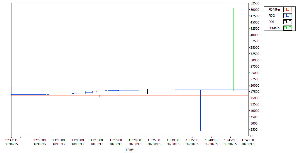
    Please find enclosed two files. One with raw data (0..65535, just 16 most significant bit without sign) and graph.

    Regards,

    Dian

  • Dian,

    I've had a quick look through your results and you have some sort of bit-wise error in your readout. I suspect this an error in how you read out the device, but without more information about how you read the data and what your system is like, I can't be sure.

    In the data file that you sent me, it looks like there are four columns of data. Columns 1-4 are labeled PDFilter, PDO, POI, and FFMain respectively. I've taken them an put them into an excel file.

    For each data, I convert this data back into hex to see what it comes from and look at the original data. Using column 1, I get data that starts at 16075 and stays there with two excursions. In the first, the device is reading 16071 for a while and for two readings, it reads 16327. For the second, it reads 16070 for a while and then goes to 15558.

    Let look at this from the hex data:

    16075 -> 16327 = 3EC7h -> 3FC7h

    16070 -> 15558 = 3EC6h -> 3CC6h

    In both cases there is a single bit error. In the first, the 8th bit read a 1 when it should have been an 0, and in the second, the 7th bit read a 0 when it should have been a 1.

    In the other columns you see similar single bit errors

    Column 2

    18185 -> 1803 = 4709h -> 070Bh

    18199 -> 1814 = 4717h -> 0716h

    Column 3

    18522 -> 2138 = 485Ah -> 085Ah

    18514 -> 16466 = 4852h -> 4052h

    Column 4

    17670 -> 16646 = 4506h -> 4106h

    17665 -> 50433 = 4501h -> C501h

    Each time it is a single bit error either changing a 1 to a 0 or a 0 to a 1. I don't know what can do this in terms of noise. I would imagine that if it were a noise issue, this has to be on the DOUT line. It can't be an SCLK issue or the remainder of the bits would be shifted.

    More likely this is some sort of readout issue where you have some sort of intermittent error. I don't know what else could cause this. My recommendation would be to try to catch this problem in the act. I'd set the input to a known value that has and then see if you can catch this with a logic analyzer.

    After that, I'd try to figure out if there's something in the code that could be flipping these bits. I really don't think this is the device that is in error. If it were the device, there would be more of a pattern (say the same bit is stuck at a 1 or 0 as an example). This has changes to high or low over any bit within DOUT.

    Joseph Wu

    Data_20151030_134943.xlsx

  • Thank you Joseph,

    Good catch, looks very logical. I will check and send you a result. Digital line between uP and ADC is not short.
    Regards,
    Dian
  • Hi Joseph,
    At datasheet, page 10/70 (timing characteristics) for tDOPD max is 50ns. There is note #3. I do not understand the note. Max is 50ns when DVDD is >3.6V OR at DVDD >3.6V tDOPD is 180ns max? What is your recommendation for DVDD? Also, recommendation for pull-up or pull-down resistor at DOUT?
    Regards,
    Dian

  • Dian,


    I'm not sure of the origin of the added note for timing for tDOPD0. I believe that the for DVDD > 3.6V, the maximum value for tDOPD is 180ms, possibly due to the effect of slew from the output drive. Regardless, this spec intends to show that the SCLK has a minimum duty cycle based on whatever SCLK frequency you use.

    I don't have a recommendation for pull-up or pull-down on DOUT. When the SPI is active, DOUT is driven to a high or low output, and neither pull-up or pull-down is necessary.

    Out of curiosity, were you able to run any tests based on my last set of comments?


    Joseph Wu
  • Hi Joseph,

    I extended the time to read DOUT. I still have some spikes, but they are every 45-50 min. Now i changed digital power from 3.3V to 5V. I will keep in touch with you.

    Regards,
    Dian
  • Dian,


    One other thing to check is the duty cycle of your SCLK lines. I just noticed that the high time seems longer than the low time in the scope plots that you originally provided. It is possible that the SCLK duty cycle is greater than 75% (even in a very rare case)? This limit is outlined in the timing requirements on page 10 of the datasheet.

    Again, I think using a logic analyzer would really help debug this problem. It might show the error with the timing information, depending on the analyzer that you use.


    Joseph Wu
  • Hi Joseph,

    Works now. The problem was - digital power. I left enough time for DOUT. With 3.3V DVDD, spike was every couple of minutes to 20-30 minutes. When I switched to 5V DVDD spikes disappears. And I did not touch the timing.

    Thank you again,

    Dian

  • Dian,


    I'm glad you were able to find the problem. Thanks for posting back the solution. If you have any other questions, please post back.


    Joseph Wu
  • Hi Joseph,

    I would like to know, why works with 5V (what is the different for the chip) and what exactly mean note #3 on page 10. I would like to understand where is my mistake to prevent future errors on my designs.

    Regards,
    Dian
  • Dian,


    I'm not sure why the device worked better with a DVDD 5V than at 3.3V. It's possible that the different supplies led to different thresholds in the error that you were seeing.

    In a previous post, I mentioned that I would remove the inductors in the supplies. I've seen cases where these inductors caused communication error (these errors were so bad that the data was completely unusable). Did you remove these inductors? These would be L3 and L4 on the schematics you had shown. They may have been a contributor to this communication error. Even on the analog side, this can cause some amount of disruption in operation. As a test, it would have been nice to short these inductors to see if these problems went away.

    As I'd mentioned earlier, I'm not sure of the origin of note 3. I'll check with others, but I don't know if I'll be able to find it. My thinking is that this note was put in because the rise time of the DOUT might get extended because of the extra slew time needed for the higher DVDD. Regardless, this would be a limitation in the SCLK timing.

    Since the device worked with a higher DVDD, it might be worthwhile to clean up DVDD to see if this helps. I would note that the scope plots for the digital communications showed a lot of noise and possible ground bounce.


    Joseph Wu
  • Hi Joseph,

    I forgot to mention to you, I removed L3 and L4. My reading is stable (I am using 18 bits without sign). I do not think the noise is an issue. The scope picture I sent you is without frequency compensated leads. I dis attached the pins from board already, but if you want screenshot I can send to you with better quality with frequency compensated leads.
    Regards,
    Dian