This thread has been locked.

If you have a related question, please click the "Ask a related question" button in the top right corner. The newly created question will be automatically linked to this question.

ADS1147 IDAC output compliance seems to be about 2.6V with 5V supply. What did I mis

Other Parts Discussed in Thread: ADS1174, ADS1147, ADS1248, ADS1148

Hi:

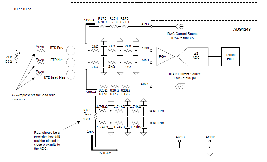
I am following the standard ratiometric design for converting RTD resistance to temperature with the high-precision reference resistor, but I am finding that the open circuit IDAC voltage measured at the chip pins is only about 2.6V with a 5V supply when asked for 500uA.  The chip was ordered through Digikey.  Is there a proper spec for the IDAC compliance somewhere?  All the graphs are "typical".

Eric Christenson

  • Eric,


    Are you referring to the ADS1147 (not the ADS1174)?


    Joseph Wu
  • Hi Eric,

    I think you meant to ask about the ADS1147. There are no IDACs in the ADS1174.

    The typical compliance voltage for the ADS1147 IDACs is AVDD - 0.7 V. With nothing connected to the IDAC output pins (i.e. open-circuit), I would expect that the pins should be pulled up to the supplies.

    Can you share a schematic of your measurement setup?
  • RTD_to_Digital.pdfMr Andrews and Mr Wu, yes, I'm a bit dyslexic, and am referring to the ADS1147!  I have attached a PDF of the relevant circuitry.  Emitter is the high-side ground plane, the SPI line drivers in both directions are isolated, and there are pullups to prevent those that can go tri-state from oscillating.

    Thanks!

  • Eric,


    For the excitation currents driving the RTD and the reference resistor, how are you routing the current? If you are routing it through the AINx inputs, you may be dropping voltage across the filter resistors. As an example, if you are routing current to AIN0, then the excitation current goes through R186, R187, and R188.


    Joseph Wu
  • OK, the circuit follows one of your app notes*. AIN3 and AIN2 are the outputs from the two IDACs, potential is measured across AIN0 and AIN1, and the output of both IDACS is routed across R183, which is used for a reference by REFP0 and REFN0.
    Thus, the current from the first IDAC goes through R173-R175, through the positive RTD lead and the RTD, and returns on the second negative RTD lead to pass through R185.
    The current from the second IDAC goes through R176-R178, throught the negative RTD lead, and returns on the second negative RTD lead to also pass through R185. The voltage drop on the outgoing negative RTD lead is the same as that going out on the positive RTD lead, so the as long as the lead resistances match, the outgoing voltage drops cancel, and the voltage across the RTD itself is the same as the voltage at the connector, where it is measured through another filter on AIN0 and AIN1.

    I am measuring the IDAC voltage at the chip pins, and it is not oscillating.

    The environment is a high-power VFD motor control (1100V, multiple hundred amps) and some high voltage, but short (1us) pulses are expected to show up on the leads. The RTD is on the main heatsink of the VFD.

    *The "application report" is SBAA201 -- March 2013, entitled "RTD Ratiometric Measurements and Filtering
    Using the ADS1148 and ADS1248 Family of Devices" by Luis Chioye. The circuit is found in Figure 10 on page 11. I have added some additional filtering in front of the IDACS, because I have had a number of RS232 driver chips without filters fail in a very similar environment.

  • Eric,

    I've redrawn your schematic so that it's closer to the figure from the application note:


    First, make sure the resistors are what they say they are. In particular, I want make sure the RTD is 100 Ohms and that the Rbias is 1 kOhm.

    Then measure the voltage across Rbias is 1V because it should be the sum of the two 500uA currents. Measure the voltage across the RTD, this should be about 50mV. And measure the voltage across R173 to R175 and that should be about 0.93V.

    The whole stack from AIN3 to GND should be about 2V. If it's less, you might have a leakage path somewhere, and if it's more, you might have the wrong IDAC current, or resistance somewhere.

    Regardless, we can use this schematic to describe voltages around the ADC. I think it's a bit easier to follow.

    Joseph Wu

  • As I said, I was cribbing the app note.

    Thank you for your help. At this point, we are barking up the wrong tree, and I found that by writing debug code and in the process comparing my original code against the datasheet.

    I am quite sure of my components...being able to both read the numbers and checking with a digital multimeter.  

    However, I missed something in the documentation, although it is in "Black and white" on page 44, where it says nnnn =number of registers to read or write (number of bytes -1).

    On the basis of that, I wrote:

    bool Write_RTD_SPI_Register_Split(uint8 reg, uint8 value)

    data = Write_RTD_SPI_BYTE(WREG|reg); // what to do starting at what register
    data = Write_RTD_SPI_BYTE(1); // how many?  (Wrong!  this writes 2 registers!)
    data = Write_RTD_SPI_BYTE(value);
    data = Write_RTD_SPI_BYTE(RTD_NOP);

    }

    The effect of this, when writing MUX0, is to write the NOOP command to VBIAS...and NOOP is 0xFF, so now I have the bias voltage connected to the analog inputs when I wasn't aware it and didn't think I was writing to VBIAS, along with other things that depend on the exact order I write to the remaining registers, including an accidental write to GPIOCFG.

    This effect is enough to make the IDAC outputs to look like they don't work correctly.

    So, documentation feedback:

    SPI COMMAND DEFINITIONS section

    Operands: subsection

    Change definition of n to read something like

    n= one less than the number of registers to read or write -- e.g. if you want to read or write one register, set n to 0.

    Thanks for the help, I now have good numbers!

    The main question remaining in my mind is whether I have sufficient filtering to ensure the ADS1147 remains reliable in an industrial switching environment.  I am debating if I should have a shield at the negative potential around the wires to the RTD.

    E.

  • Eric,


    I'm glad you were able to figure out your problem. I thought it wouldn't take to long to debug this one.

    When it comes to the shielding, I would definitely consider it. Really, I think that you should always consider problems like this in the layout of the pcb. It's hard to get right, but minimizing loops in the signal path will really help limit the EMI/RFI pickup. Filtering will help too, but layout is a big factor.


    Joseph Wu