This thread has been locked.

If you have a related question, please click the "Ask a related question" button in the top right corner. The newly created question will be automatically linked to this question.

Need help with Dac39J82 JESD link establishment.

Other Parts Discussed in Thread: DAC39J82, DAC38J84, LMK04828

Hi,

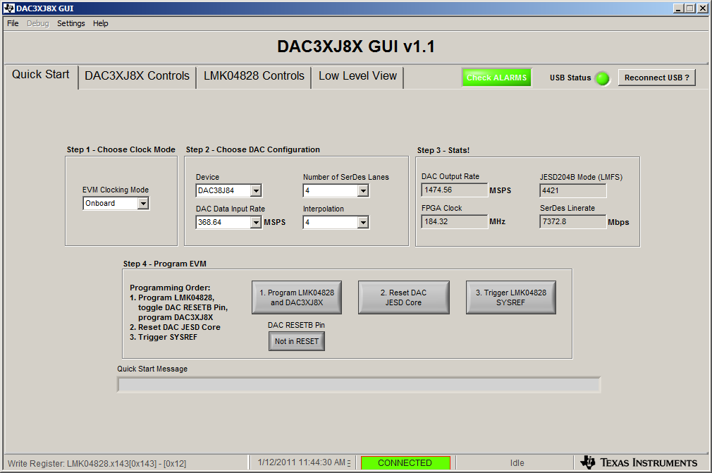
I am trying to establish the JESD link between Dac39J82 and FPGA. I am following the Initialization set up sequence at page 132 of the DAC39J82 specs.

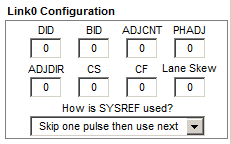
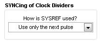
After I feed in a single Sysref pulse, (and I did make sure this pulse happened by monitoring it on the oscilloscope), I did not see the Sync signal come out from the SYNCB pin of the Dac. I have been stuck for a couple of days. Can anybody throw some lights on this?

Thanks a lot.

Hao

  • Hi, Hao:


    1> For the polarity of SYNCB, when the DAC38J84 is requesting sync, the SYNCB (LVDS logic) is set to logic LOW. The FPGA then will send the K28.5 characters. When CGS is established, then the SYNCB will rise to LVDS logic HIGH. Please kindly check the SYNCB signal is High ->Low  in your case?

    2> By default, the GUI will set JESD204B to skip one SYSREF pulse than use the next pulse as below:

    So, if you send only one SYSREF pulse, it is not sufficient, because only the clock divider is synced as below:

    3> The reason that you may use multiple pulse is that in the DAC logic, there is a clock divider circuit that provides all the divided down clocks to the digital logics and all the JESD logics. The clock divider is initialized by the SYSREF upon the first pulse. We thus set a delay on the JESD logics to use the next pulse of SYSREF to ensure the divided down clocks are initialized properly prior to the JESD link sync.

    4> Once again, upon powering up of the DAC38J84, the SYNCB LVDS logic will output logic HIGH. After the programming of registers, the initialization of JESD block, and triggering of the SYSREF, the SYNCB LVDS logic will output logic LOW to request JESD synchronization/CGS stage from the FPGA. If SYNCB stays low, it means that your CGS stage haven't been passed.

    5> You may try the SYSREF with several pulses, normally, we use 8 SYSREF pulses.

    6> For the startup sequence, please kindly refer to the attachment:

    8030.DAC38J84 Start-up Sequence.docx

    Thanks a lot!

    Yarn.

  • Hi, Yarn,

    Thanks a lot for your reply. I really appreciate it. I followed very closely the Start-up sequence you posted when you replied to me, but I still can not make SYNCB signal line goes to low in the first place, (not to mention it goes back to high to pass GCS stage). I have been stuck for more than a week, I am very grateful for your enlightment. Thanks a lot.

    I will post my register settings below, can you tell me what could be possibily wrong with my sequency of register settings. I am generating 4 sysref pulse from LMK04828. For DAC39J82, I use "skip one SYSREF pulse and then use only the next pulse" for clock divider initialization. I use"skip two SYSREF pulses and then use only the next pulse ", which is the example for pulsed SYSREF in the document u posted. Below is my sequence.

    1) Initialize LMK04828 to feed in DACCLK to the DAC39J82.
    2)set RESETB pin to low and then high to reset the SIF register while keeping the TXENABLE pin to logic low.
    3) do the following DAC39J82 register settings, the first parameter is the SPI slave select bit, the second parameter is register number, third parameter is the register value:

    write_dac39j82_reg(ss, 0x02, 0x2002);
    write_dac39j82_reg(ss, 0x02, 0x2003); // LSB: A transition from 0->1 causes a reset of the SIF registers.
    write_dac39j82_reg(ss, 0x4A, 0x001E); //put JESD into init_state, in this mode, JESD can be programmed

    write_dac39j82_reg(ss, 0x00, 0x0118); //set to 2x interpolation, disable QMC.
    write_dac39j82_reg(ss, 0x02, 0x20D2); //turn on full complex mixer, and set SPI to four wires mode.
    write_dac39j82_reg(ss, 0x14, 0xAAAB); //Low 16bits of NCO Frequency adjust word for DAC AB path
    write_dac39j82_reg(ss, 0x15, 0xAAAA); //middle 16bits of NCO Frequency adjust word for DAC AB path
    write_dac39j82_reg(ss, 0x16, 0x682A); //upper 16bits of NCO Frequency adjust word for DAC AB path
    write_dac39j82_reg(ss, 0x1A, 0x0005); //DACB and DACD into sleep mode, enable DAC PLL.
    write_dac39j82_reg(ss, 0x22, 0x1B27); //using DACA for I and DACC for Q.

    write_dac39j82_reg(ss, 0x24, 0x0030); //Determine how SYSREF is used to sync the clock dividers in the device, Skip one SYSREF pulse then use only the next one.

    write_dac39j82_reg(ss, 0x25, 0x6000); //JESD clock divider to 8, we do not understand but from TI forum.
    write_dac39j82_reg(ss, 0x31, 0x0408); //use PLL output to be DAC rate (not bypass PLL), set N divider to 2. set lock detector window to be most narrow.
    write_dac39j82_reg(ss, 0x32, 0x0300); //set PLL M divider to be 4, Prescaler to be 2.
    write_dac39j82_reg(ss, 0x33, 0x67B0); //select H band VCO, Sub-Band 5266.2-5277.1MHz, CP 600uA.

    write_dac39j82_reg(ss, 0x34, 0xC000); //SYNCB OUPUT current set to high.

    write_dac39j82_reg(ss, 0x3B, 0x1800); //select from DACCLKP/N 1320MHz,
    write_dac39j82_reg(ss, 0x3C, 0x9228); //enable div by 80
    write_dac39j82_reg(ss, 0x3E, 0x0108); //full operating rate, lane rate =
    write_dac39j82_reg(ss, 0x4A, 0xFF1E); //turn on all 8 serDes lane, put JESD into init_state, in this mode, JESD can be programmed and its ouputs stays at zero
    write_dac39j82_reg(ss, 0x4B, 0x1F00); //set JESD elastic buffers to 32 (same as frames per multi-frame), set octets per lane per frame cycle to 1.
    write_dac39j82_reg(ss, 0x4C, 0x1F07); // 32 frames per multiframe, 8 lanes used by JESD.
    write_dac39j82_reg(ss, 0x4D, 0x0101); //2 converters per link. 2 samples per frame per converter.
    write_dac39j82_reg(ss, 0x4E, 0x0F4F); //set High Density mode for the JESD. When asserted samples are split across lanes..
    write_dac39j82_reg(ss, 0x51, 0x0000); //select which errors cause a sync request, disable the sync request.
    write_dac39j82_reg(ss, 0x5C, 0x1155); //Determine how SYSREF is used in JESD synchronizing block. Skipe two SYSREF pulse and then use the next SYSREF pulse.
    write_dac39j82_reg(ss, 0x61, 0x000D); //select which link sync_n outputs are anded together to generate syncB LVDS output.

    //clear SerDes PLL "out of lock" bit
    write_dac39j82_reg(ss, 0x6C, 0x0000);
    //A rising edge causes the error_cnt for link0 to be cleared
    write_dac39j82_reg(ss, 0x5C, 0x11DD);
    write_dac39j82_reg(ss, 0x5C, 0x1155);

    //start the JESD link initialization, TI recommends the set JESD to exit out of the reset state first, then set JESD to exit out of the initialization sate.
    write_dac39j82_reg(ss, 0x4A, 0xFF1F);
    write_dac39j82_reg(ss, 0x4A, 0xFF01);

    4) generate 4 pulses of SYSREF from LMK (I did see the four pulses on the SYSREF input pin of the DAC39J82 on the oscilloscope)
    5) I should expect to see the SYNCB goes low and then goes high, but I did not the SYNCB goes low in the first place.
    6) set TXENABLE pin to logic high.
    7) int BID = read_dac39j82_reg(ss, 0x50); //read bank ID
    int DID = read_dac39j82_reg(ss, 0x51); //read Device ID
    I read all zeros back, (I should read back some value I plugged in the FPGA before)


    Thanks a lot. Can you tell me what could go wrong?

    Hao
  • Hi, Yarn,

    If what I replied is too much, as an alternative, if possible, can you show me all your DAC39J82 register settings of your start-up sequence? I am not sure whether it is the hardware or the register settings of my start-up sequence right now that make it not work. So If I can verify my register settings of start-up sequence with yours, I can cut the problem and chase the right direction.

    Thanks a lot, your help is greatly appreciated.

    Hao
  • Hi,Hao:


    I have checked  your configuration procedure, and may find these points from my sight of view:

    1>when pulsed SYSREF is used, make sure SYSREF is DC coupled.

    2>SLEEP pin should be low, because by default config 35 is 0xFFFF, which means SLEEP pin directly routed to various blocks of DAC.

    3>If JTAG is not used, make sure TRSTB pin is low.

    4>Regarding register 0x61, if only link0 is used, 0x001 or 0x211 is suggested, by default, we set it to 0x211.

    5>For the BID and DID value you mentioned, I tried with my setup and get all zeros. I think you can ignore it as datasheet says.

    6>To test the DAC, you can refer to ATEST pin and try register config27.

    7>I think your setting of 'SYSREF arming' and 'JESD block reset' is right. Firstly,   JESD block should be reset and set to INIT_STATE. Then using the second SYSREF pulse to sync clock divider and using the third SYSREF pulse to sync JESD block. After JESD block is synced, SYNC is pulled low(I probed it in my setup). Then JESD link begin the CGS stage.

    8>I have attached my setup snap and configuration file for your information. Hopes it can help you.


    DAC3xJ8x start up configure.xlsx

    Thanks a lot!

    Yarn,