This thread has been locked.

If you have a related question, please click the "Ask a related question" button in the top right corner. The newly created question will be automatically linked to this question.

Correct operation for ADS1240

Other Parts Discussed in Thread: ADS1240, ADS1220


Dear Technical Support Team,


I have some questions about ADS1240.
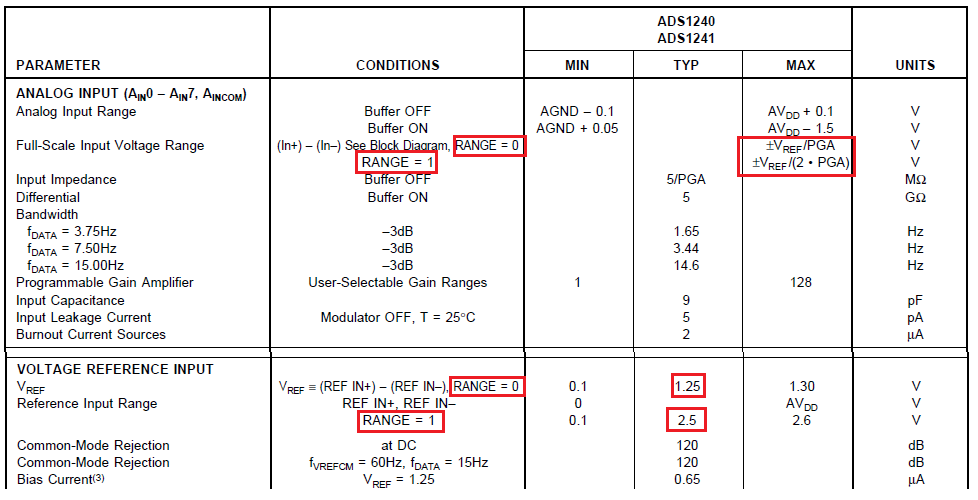
 

1.)

Datasheet shows following specs for AVDD=3V.


Dose it means that input fullscale range always 1.25V?

RANGE = 0 ±VREF/PGA V ←Vref should be 1.25v on datasheet. PGA=1

RANGE = 1 ±VREF /(2 • PGA) ←Vref should be 2.5V on datasheet. PGA=1


Customer's condition is following and they would like to input 2.5V full-scale.

AVDD=3.3V、VREF=2.5V、RANGE=1、PGA=1、between Ain1 and AinCOM(GND)、format=unipolar


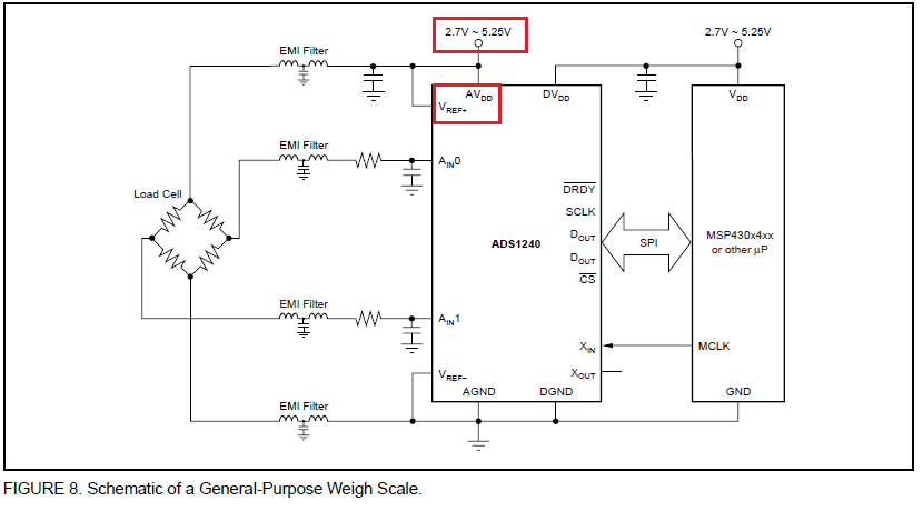
Following shows "FIGURE 8". It connect same voltage for AVDD and Vref.

Is Vref over voltage(such as 2.7V and 5.5V) for datasheet spec?


Best Regards,

y,i

  • y.i.


    1. I believe that with AVDD, it forces the input full scale range to be 1.25V. As you mentioned in a previous post, there is a section that says:

    For AVDD = 3.0V and RANGE = 0 in the ACR, the differential VREF must not exceed 1.25V.
    For AVDD = 3.0V and RANGE = 1 in the ACR, the differential VREF must not exceed 2.5V.

    With the ADS1240, I don't believe that at AVDD=3.3V and VREF=2.5V the input full scale range will reach 2.5V full scale.

    2. I'm not sure of the figure, but it would only work for the case where AVDD=5.0V and RANGE = 1. In that example, you would still be limited to a full-scale range of 2.5V.

    I'll check to see if the design group has any comments on the the reference limitations, but at this point I don't think the ADS1240 will work for the desired application.

    However, is your customer willing to consider an alternate part? The ADS1220 could work with AVDD=3.3V, VREF=2.5V, with the desired full-scale range.

    If they may be interested, they can download a datasheet here:

    www.ti.com/.../ads1220.pdf


    Joseph Wu
  • Hi Joseph,

    Thank you for your reply.

    >I'll check to see if the design group has any comments on the the reference limitations,
    >but at this point I don't think the ADS1240 will work for the desired application.
    ⇒If possible , could you check above for 2.5V full-scale range with AVDD=3.3V?  

       Customer can get expected result with following settigns, so they would like to use it.

        But it dosen't much datasheet spec , expecailly Range=0 dosen't allow exceed VREF=1.25V.

       AVDD=3.3V、VREF=2.5V(+Vref=2.5V / -Vref=0V)、RANGE=0、PGA=1、Ain1(data)-AinCOM(GND)
     
    Best Regards,
    y.i

  • y.i.


    I've checked with the designer about this part and the problem is the sample charging when the reference is at a higher voltage.

    If the reference voltage is too high, then the sampling within the delta-sigma modulator may have charges that go higher than the supply. If this happens, then the charge leaks from the modulator. Since this is part of the reference sampling, I'm not sure if you see the charge equally through the input range, but it's likely you would see a very large gain error and integral non-linearity.

    I would have them look at different input voltages (measured with a precision multimeter) and see how much of an error there would be. I suspect that this error would be worse at higher temperatures.

    Regardless, his recommendation was the same as the datasheet. Do not run the device with such a high reference and RANGE=0. Use RANGE=1.


    Joseph Wu
  • Hi Joseph,

    Thank you for your reply.
    I understand that we should avoid to use Vdd=3.3V and Vref=2.5 and Range=0 for 2.5V FS.
    I suggest following to the customer for 2.5V FS.

    a.) Vdd=5V , Vref=2.5V , Range=0
    b.) Vdd=5V , Vref=5V, Range=1
    c.) ADS1220 with AVDD=3.3V, VREF=2.5V

    Best Regards,
    y.i