This thread has been locked.

If you have a related question, please click the "Ask a related question" button in the top right corner. The newly created question will be automatically linked to this question.

wrong ads1248 reading value and SPS setting

Other Parts Discussed in Thread: ADS1248

Hi, 

Before I used the ads1248 chip to measure the 3 RTD100 temperature signals in my old board. I used the 3 differential inputs and the 4-wire RTD interface.

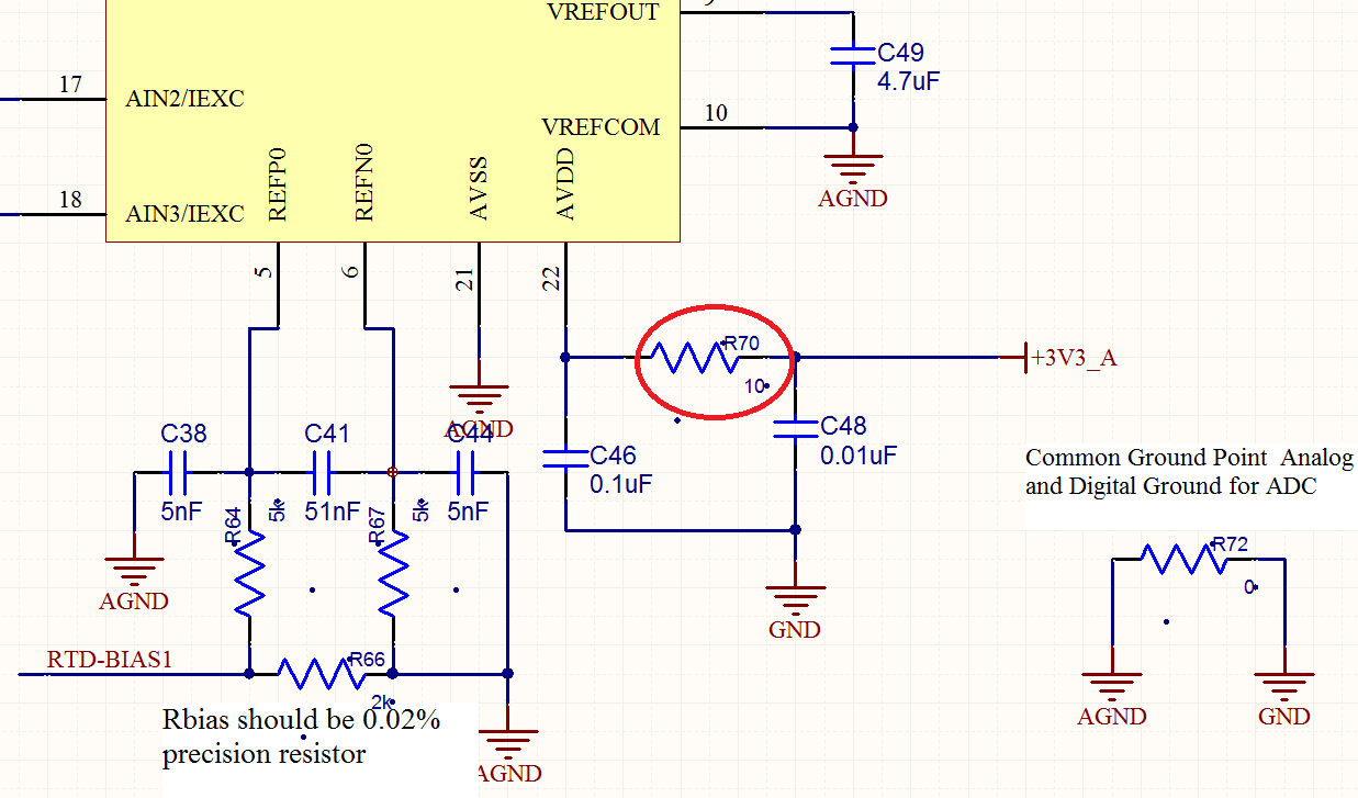
The following was some important configuration:

Excitation Current: 250ua

PGA:16

SPS:80

Rbias:2K

The old board is good.

Now I use same design in my new board. There are two ads1248 chips because I want to measure 6 temperature signals.

I can read the digital code from ads1248. I will get a sampling value every 1/3 second, So I will sample all three channels in one second.

But some error in the reading value. Normal value should be 7235XXX, the real value is 7516XXX.

When I change the SPS value, the reading value will change too.

SPS=80, Reading value=7516000;

SPS=320, Reading value=7235000;

SPS=1000, Reading value=7106000;

(1) I want to know how to select a SPS setting value, why the reading value changes if changing the SPS value.

(2) when to calibrate the ads1248 chip? only after power on, or each time I switch to a new channel?

Thank you

  • Fei,


    Are you cycling through the three readings? My guess is that you have extra capacitance on your input or reference that is slowing the settling in the RTD or reference resistor. While setting the excitation current to a new pin is relatively instantaneous, the filtering capacitors that you have (or other external capacitance) will still need to charge or discharge, depending on the set up.

    I would try an experiment. Make the 3 measurements by taking one sample each. Then, do the same thing by taking 20 measurement each before moving to the next channel. Do the values change between the different reads? Does it look like the measurement is settling with the 20 consecutive measurements?

    Then look for capacitances or resistances on your schematic that cause RC time constants that might make the difference in what you see for the different data rate readings. If you need some help, feel free to post the schematic here.

    I might also try removing some of the input or reference capacitors on the board to see if this helps. You may need to add some delay into the channel cycling to get measurements that are more accurate.

    As for the calibration, the ADS1248 is factory-trimmed for gain for each of the PGA settings, which is set each time the PGA is setup in the device. In this case, a gain calibration is probably not necessary. As for the offset calibration, we've said that a calibration should be done after powering on, a change in temperature, a change in PGA or sometimes a change in channel. This depends on what sort of offset that you are willing to accept. It's likely that if you keep the same gain, you could just set the PGA and live with any offset drift that you might see after the calibration.


    Joseph Wu
  • Hi, Joseph,

    Thank you for your detailed answer.

    Now my ads1248 chip works correctly. The problem is from the hardware. The voltage on the AVDD pin is not 3.3V, it is a little lower voltage.

    A bigger or smaller AVDD voltage will change the sampling result? It is strange. OK, do not care for it.

    Now If I change the SPS value, the sampling value will not include a big error. It seems the error gets smaller when using a bigger SPS value.

    I did not do the gain calibration. About the offset calibration, it is done only when power on.

    Another question is that how to detect if a RTD sensor is in the connector or not?

    Thank you

    Fei
  • Fei,


    I'm glad that you were able to get it to work. I'm a little surprised that the problem was that the AVDD was a little lower than expected. How low was the value?

    There are some small differences in operation with different AVDD. This includes the noise (which is shown in Tables 1-6), the PSR, which is explained in the Electrical Characteristics table, and power supply current shown in the Typical Characteristics curves. All of these are relatively minor effects and I don't think it should significantly affect your performance. I would note that with a low analog supply, you need to be careful on selecting your RTD, reference resistor, and the excitation current. The compliance voltage for the excitation current only goes to AVDD-0.7V.

    If there is no RTD sensor in the connector, it is likely that the AINP will be pulled up by the excitation current source, and the AINN will be pulled low from the lack of current going to the reference resistor. In this case, I would expect that the ADC would over range and give you a full scale reading of 7FFFFF. If you need any other evidence, you can use the system monitor and use the internal reference to read the external reference value (either pins to REF0 or REF1). If the reference reads 0, the excitation current isn't going through the RTD to the reference resistor.


    Joseph Wu
  •  

    Hi, 

    This is a old design. It can work in the old design.

    Please look at the resistor R70. In this design its value is 10ohm/1%. I can not understand it. I think it should be 0ohm.

    In my old boards, this resistor can be 10ohm/1% or 0ohm. They can work correctly.

    I removed a R70 resistor from the new boards, I found it is about 15 ohm. Then I got the bad measurement.

    Then I changed it to 0 ohm, everything is good.

    Fei

  • Fei,


    I'm glad that worked for you, but I'm not sure that was exactly the original problem. I think the original intent was to low pass filter the supply to make sure the supply was well behaved. Since the supply current is typically lower than 500uA (or equal to that at the highest data rates), there isn't going to be much drop across this resistor (only 5mV with the 10Ohm resistor).

    Anyway, if the device is now working. I can't argue with it. Let me know if you have any other questions.


    Joseph Wu
  • Joseph,

    My sensor detection works too. Just measure the external reference voltage based on the onboard reference.

    The temperature sampling is perfect now. The sampling period is 1 second.

    MCU>5:TEMP$7238421, 7255391, 7247870, 0, 7257150, 0
    MCU>5:TEMP$7238500, 7255439, 7247965, 0, 7257167, 0
    MCU>5:TEMP$7238576, 7255454, 7247959, 0, 7257176, 0
    MCU>5:TEMP$7238576, 7255449, 7248020, 0, 7257223, 0
    MCU>5:TEMP$7238627, 7255493, 7248052, 0, 7257202, 0
    MCU>5:TEMP$7238681, 7255522, 7248018, 0, 7257200, 0
    MCU>5:TEMP$7238683, 7255543, 7248021, 0, 7257242, 0
    MCU>5:TEMP$7238700, 7255558, 7248015, 0, 7257224, 0
    MCU>5:TEMP$7238731, 7255644, 7247996, 0, 7257227, 0
    MCU>5:TEMP$7238799, 7255662, 7248004, 0, 7257236, 0
    MCU>5:TEMP$7238846, 7255674, 7248049, 0, 7257227, 0
    MCU>5:TEMP$7238885, 7255644, 7247998, 0, 7257241, 0
    MCU>5:TEMP$7238997, 7255605, 7247992, 0, 7257229, 0
    MCU>5:TEMP$7239116, 7255616, 7247962, 0, 7257194, 0
    MCU>5:TEMP$7239184, 7255547, 7247941, 0, 7257205, 0
    MCU>5:TEMP$7239232, 7255536, 7247948, 0, 7257226, 0
    MCU>5:TEMP$7239304, 7255498, 7247961, 0, 7257176, 0
    MCU>5:TEMP$7239404, 7255467, 7247934, 0, 7257209, 0
    MCU>5:TEMP$7239438, 7255428, 7247948, 0, 7257184, 0
    MCU>5:TEMP$7239477, 7255429, 7247903, 0, 7257198, 0

    Thank you very much.

    Fei
  • Hello,

    I found another problem about the ADS1248 temperature measurement for a long-time reading. the reading value will give a big jump sometimes.

    the schematic and parameter configuration have been listed in the above posts.

    (1) Test 1: initialize ADS chip, select the 1st channel and write register, calibrate offset, start converter, wait, read the digital values one by one with sampling interval 150ms.

    7300218 169
    7300113 -105
    7300212 99
    7300025 -187
    7299922 -103
    7300147 225
    7300110 -37
    6747728 -552382
    7299923 552195
    7299858 -65
    7299971 113
    7299977 6
    7300258 281
    7300162 -96
    7300126 -36
    7300016 -110

    In this table, sampling values are listed in the first column, sampling transitions are listed the second column. A big negative transition occurs. Then the next reading value become normal.

    What will lead to this big transition? I do nothing on the ADS chip except reading digital values every 150ms.

    (2) Test 2:  initialize ADS chip, select the 1st channel and write register, calibrate offset, start converter, wait, read the digital values one, same operation for the 2nd channel, same operation for the 3rd channel, go back to the 1st channel......

    I will do a new offset calibration when switching to next channel. I will get a big reading transition too.

    (3)  As for calibration discussed before, a calibration should be done after powering on, a change in temperature, a change in PGA or sometimes a change in channel.

    As I understand, "a change in temperature" should be the change in environment temperature.

    What means "a change in channel"? I should calibrate the offset register or not? when I switch to a different channel.

    Thank you

    Fei

  • Fei,


    First, I think the problem is that you are reading the data asynchronously without using the /DRDY to trigger the read. If you read the data without checking when the /DRDY occurred, then a new conversion completion can interrupt your read. For example, looking at the data, I'll select the points around the error. Here are 5 data, with the error in the middle.

    7300147 6F6433h
    7300110 6F640Eh
    6747728 66F650h
    7299923 6F6353h
    7299858 6F6312h

    The first column is the raw data, the second column is the hex conversion. In the third data, you start to read the data, but you get out the first four bits to be 0110 (6h). Then you are interrupted by a /DRDY in the middle of the read. This will update the DOUT register on the device and it will start over because there has been a new conversion. It then follows with the remaining 20 bits (6F650h) and you never clock out the last four bits of the new conversion.

    I talk about this happening in an old blog that I wrote that can be found here:

    e2e.ti.com/.../help-i-can-t-talk-to-my-data-converter-what-s-wrong

    This is shown in the description for Figure 3. If you want to avoid this, you must either trigger the read from the /DRDY (and read out the data before the next /DRDY), or you can put the device in SDATAC mode. In SDATAC mode, you can read the data with an RDATA command, and you will not be interrupted by a new conversion.

    Generally, you won't have to do another calibration for a change in the channel (this would be for different settings of the input multiplexer of the device). I've never seen a case where this is necessary. The calibration will usually correct for offset and gain errors in the ADC and PGA. Because the multiplexer doesn't usually add much error from channel to channel, I don't think this has been commonly done.


    Joseph Wu
  • Hi, Joseph Wu,

    Thank you very much

    Fei