This thread has been locked.
If you have a related question, please click the "Ask a related question" button in the top right corner. The newly created question will be automatically linked to this question.
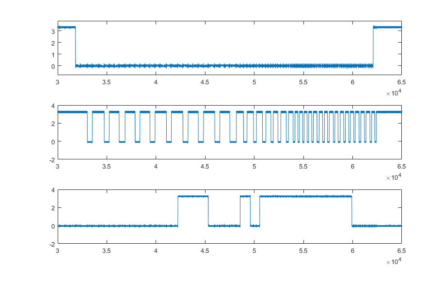
Trying to program the DAC8568 using SPI with no luck. The attached image shows the SYNC_,SCLK, DIN lines (from top to bottom) for an attempt to sequentially program Channel C to full output, note that the entire window shown is about 100ms. For reference, LDAC_ is tied to ground, CLR is high, Vref is 1.65V (with 0.22uF cap to ground) and AVdd is 3.3V (with 1uF cap). The waveforms look clean enough to me, but the DAC8568's output doesn't seem to change from 0, which is the startup condition.
Howdy Spartan,
Can you provide the timebase for the x-axis, as well as the values you are trying to write to the device? I'm also curious about the phase shift of SCLK during communication, is it meeting the timing requirements specified in the datasheet? The image is difficult to read, but I think I see 33 clock falling edges within the active sync -- you will need 32 valid clocks for proper communication.
Best Regards,
Matt
Thank you for taking a look at this, to answer your questions:
The duration of the SYNC_ being pulled low is about 100ms, so maybe 3us per plotted data point. I am using Example 2 from the documentation (www.ti.com/.../dac8568.pdf) with DATA being all ones. Thus, I am expecting to be shifting in the register values of 0000 0011 0010 1111 1111 1111 1111 0000. There are indeed 33 clock falling edges, the last one occurs after the SYNC_ is pulled high (and I think the documentation says any edges beyond the first 32 bits are ignored). Attached is the raw data I captured in case the figure was too low-resolution. I'm not seeing any phase requirements on the datasheet, there are some minimum timings, but they're all in tens of nanoseconds.