Because of the holidays, TI E2E™ design support forum responses will be delayed from Dec. 25 through Jan. 2. Thank you for your patience.

This thread has been locked.

If you have a related question, please click the "Ask a related question" button in the top right corner. The newly created question will be automatically linked to this question.

DAC5686 register settings

Other Parts Discussed in Thread: DAC5686

Dear TI team,

We are using DAC5686 in one of our design,


We have an input clock frequency of 80 MHz and the data is not interleaved. A 160 MSPS DAC update rate is desired.

For this mode, we can use DIV = 2x assuming the VCO and LPF are optimized around 320 MHz and SEL is set to 2x.


We have generated 10MHz as message frequency with 80MHz Data clock as sampling frequency.


For this we have used following register setting

                                                                                                                                x"0F00",--dacb_offset_gain_msb

                                                                                                                                x"0E00",--dacb_gain_lsb

                                                                                                                                x"0D00",--dacb_offset_lsb

                                                                                                                                x"0C00",--daca_offset_gain_msb

                                                                                                                                x"0B00",--daca_gain_lsb

                                                                                                                                x"0A00",--daca_offset_lsb

                                                                                                                                x"0900",--config_usb[see PLLVDD]

                                                                                                                                x"0710",--config_lsb[mode-dualdac,div-1x,sel-x2,counter-disable,full_bypass-disabled]

                                                                                                                                x"0600",--phase_msb[15:8]

                                                                                                                                x"0500",--phase_lsb[7:0]

                                                                                                                                x"0400",--freq_msb[31:24]

                                                                                                                                x"0300",--freq_umidsb[23:16]

                                                                                                                                x"0200",--freq_lmidsb[15:8]

                                                                                                                                x"0100",--freq_lsb[7:0]

                                                                                                                                x"0000",--chip_ver

                                                                                                                                x"0803"--config_msb[sif4, 2'complement]


But the output is not clean and Output level is very low <10 mV. We have also monitored PLLLOCK which is locked.


Is any thing I need to change in the register setting. please suggest me any other changes required to get clean output.

regards,

syed

  • Syed,

    I will look into this either today or tomorrow.

    -Kang
  • Syed,

    Your 0x0f register and 0x0B, 0x0C, 0x0E, and 0x0F registers are all programmed 0x00. This indicate the DAC A and DAC B gains are all set to 0. There will be no output full-scale current at all and explain the low amplitude output.

    Please program daca_gain(11:8) and dacb_gain(11:8) to be 2b'1111 for a full-scale current output. I.e. 0x0C = 0x0F and 0x0F = 0x0F.

    -Kang

  • Hi Mr. Kang

    Thanks for your quick response,

    I have set 0x0C and 0x0F register to value x0F, now I'm getting an amplitude 200mV pk-pk, but the required frequency is not coming.

    I had set input clock rate of 80 MHz and the data 10MHz but data frequency is coming around 8.9MHz and varying.

    I had also set input clock rate of 80 MHz and the data 8MHz but data frequency is coming around 7MHz and varying.

    Is there any other registers required. I have referred Application Report SLWA040A PLL Mode EXAMPLE 3.

    --

    Vivek


  • Vivek,

    My understanding is that your PLLLOCK is in logic HIGH indicating your PLL is locked. To make sure your internal clocking are done correctly without any frequency error, do the following:

    1. tri-state the CMOS data output from your FPGA. The DAC5686 CMOS DA and DB inputs have internal pull-down, so the input code will be 0s.

    2. make sure config0x08, bit 0 (twos) is set to 2b0 for offset binary. The input will be full-scale negative.

    3. enable the Fdac/4 mode in SSB or Quadrature mode. You should see 80MHz out of the DAC. (you can also use the NCO frequency to adjust the output further if you would like).

    If the output frequency is expected, then the internal clocking is correctly. There may be some thing wrong on your data input pattern. 

    You may also download our HSDC PRO GUI, generate the tones in the GUI under the DAC panel, and save the tone as a .csv file. You may load the I/Q signal back to your platform to double check for signal frequency.

    -Kang

  • Hi Kang,

    I have made changes, you have given and now i'm getting DAC output frequency correctly,

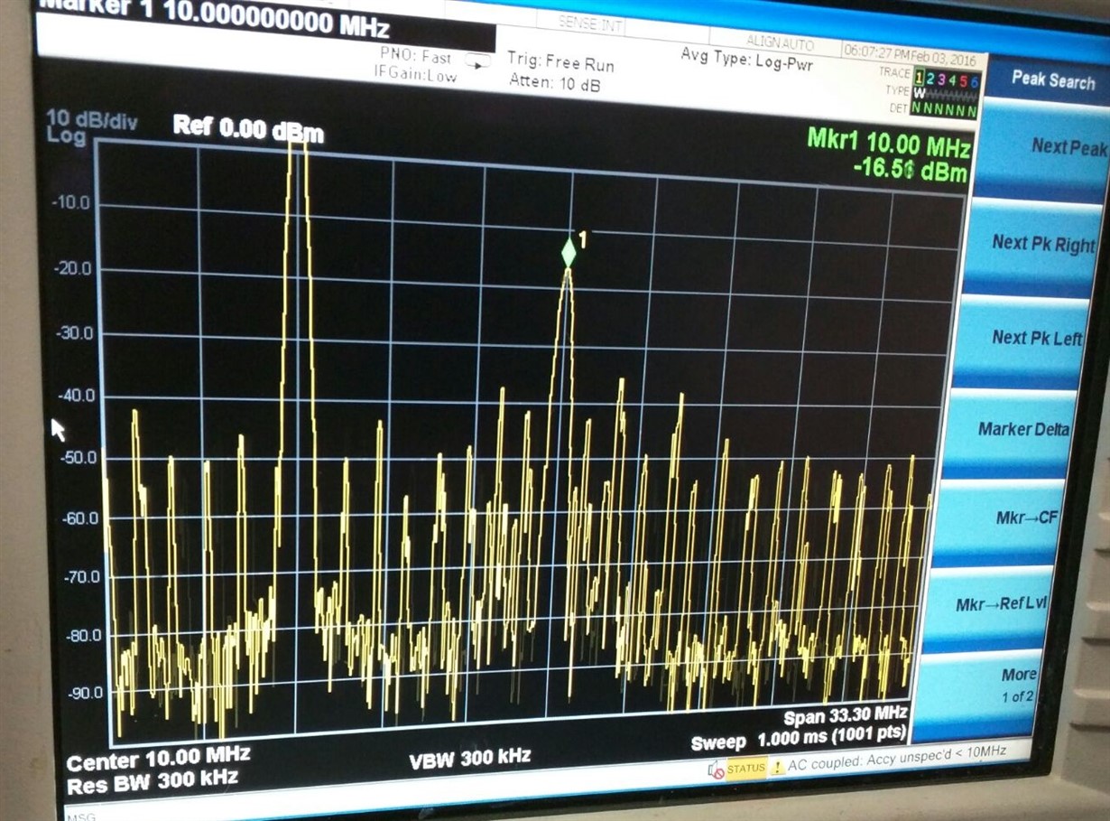
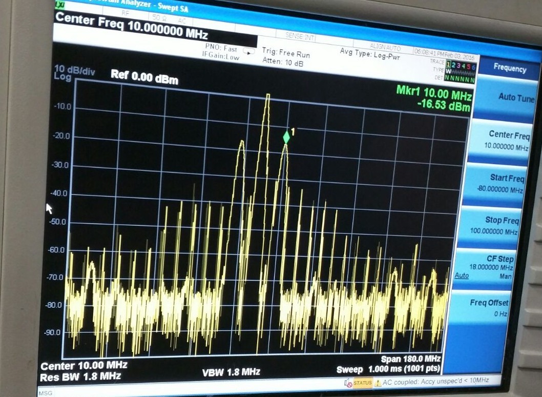
    but output noise floor is more.

    1. I'm working in PLL Mode Non-Interleaved Data , CLK1 and CLK1C (80MHz).

    2. Data input pattern on DA[15:0] and DB[15:0] I'm feeding 10MHz generated on same 80MHz sampling which i'm giving to CLK1 and CLK1C.

    3. I have monitored Clock CLK1 and CLK1C fed to DAC5686 is clean without any frequency error.

    I'm attaching with the images captured in Spectrum Analyzer showing 10MHz single tone frequency.

    --

    Vivek V

  • Vivek,

    I have a couple of thoughts

    1. Please double check your input pattern matches the corresponding input pattern programmed in register 0x08 (twos). There are two options: twos complement and offset binary format. 

    2. It is possible that the upper most significant bits are programmed correctly while the lower bits are not in your input pattern. If the lower bits are not programmed correctly, the bit error could cause these spurs.

    3. Do you have any switching power supplies (DC/DC converters) running that matches the offset spur frequencies that you are seeing. Any switching frequency on the power supply line will directly modulate onto the output signal and potentially create a double side band spurs like what you are seeing. Pay attention especially to the PLLVDD

    4. Check the power supply level on DVDD rail to make sure it is around 1.8V. This is the digital rail, and if the voltage drop caused by power supply filtering is significant, the DAC digital logic could run into speed issues, and cause spurs like you see.

    -Kang