This thread has been locked.

If you have a related question, please click the "Ask a related question" button in the top right corner. The newly created question will be automatically linked to this question.

ADS1255 self calibration is not working as expected

Other Parts Discussed in Thread: ADS1255

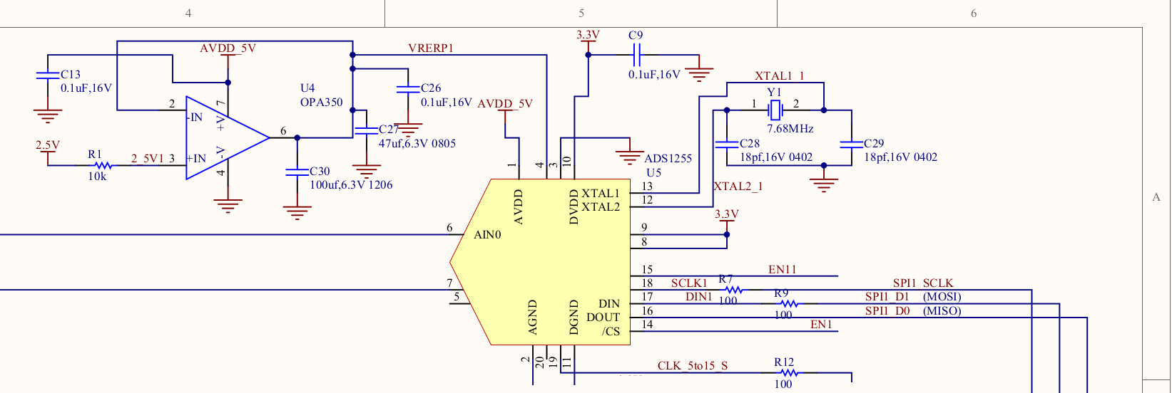
I'm trying to debug my ADS1255s (I have 4 on the same board with daisy-chained 7.68MHz clock signals but the diagram will just show one of them) as they have been reporting incorrect voltages when presented with a known input.


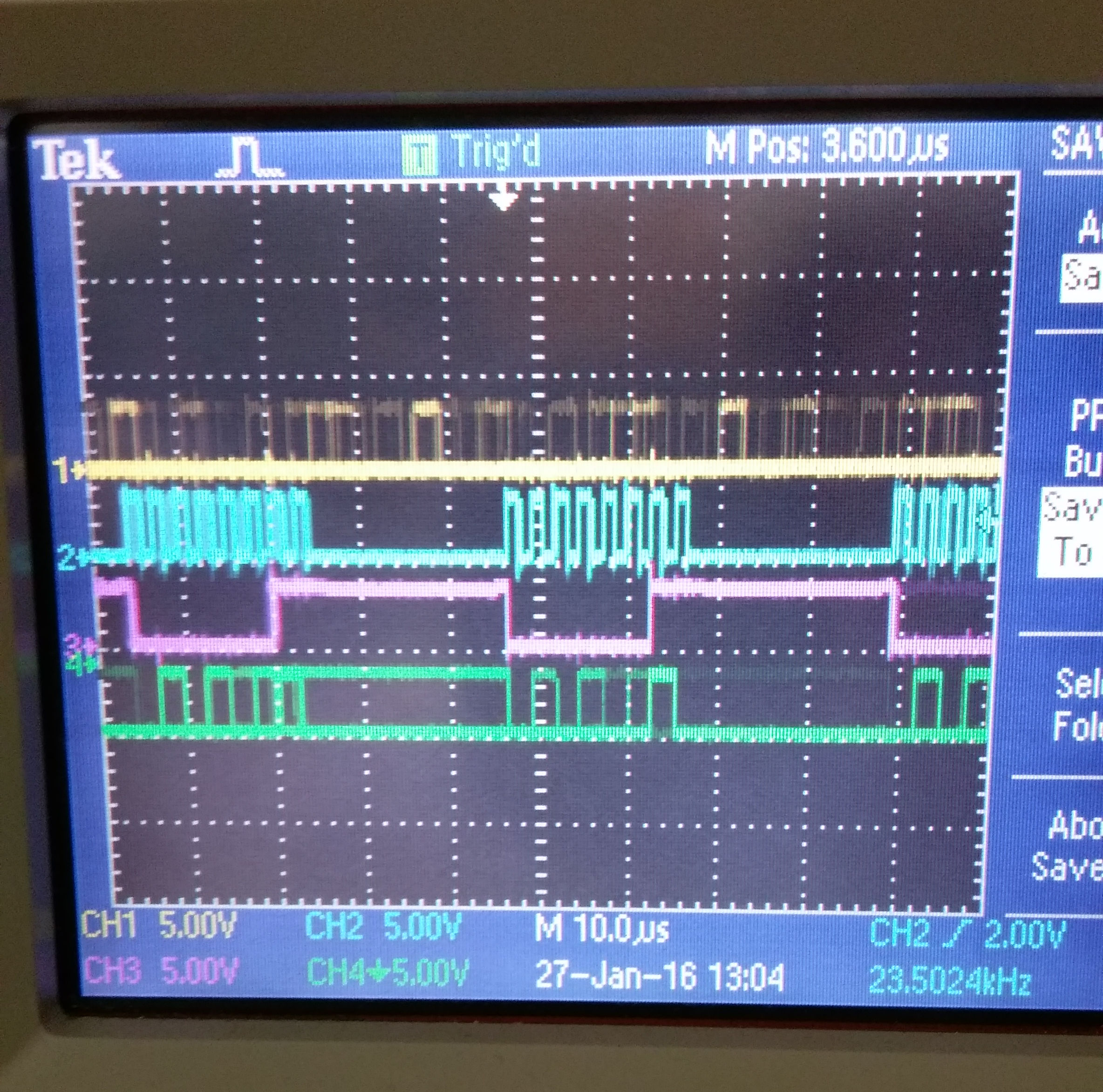
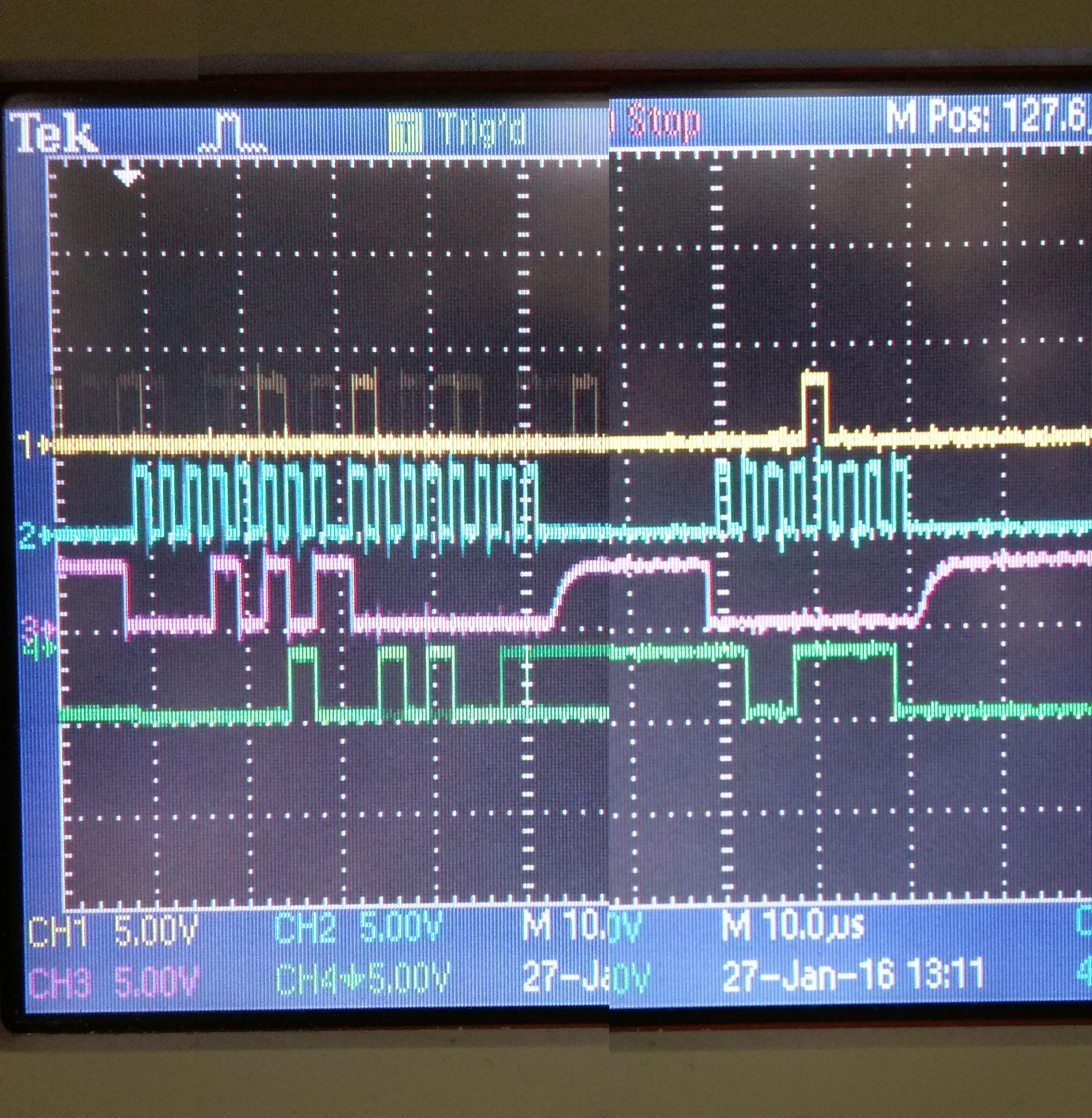
Right now I am seeing that the number I get out when presented with alternating 5v (= full scale = 2 x VREF = 2 x 2.5) and 0v differential signals is wildly incorrect after performing a self calibration. Here are 3 measurements taken sequentially about 300ms apart.

5V signal
=========
626072h : 3.842842v
6260E4h : 3.842910v
627FF7h : 3.847651v

0v signal
=========
FDFFAFh : -0.078173v
FDFDFCh : -0.078433v
FDFDFEh : -0.078431v


If I instead perform a SYS[G/O]CAL with a 0v and 5v input, I get something a bit more respectable. Pragmatically though I cannot perform such calibrations as I have no way to provide reference signals without getting my hands dirty or redesigning the circuit board. I would've imagined SELFCAL to be apt enough to at least get measurements to within 100mV?


My control flow is as follows:

[COLD BOOT]
WAKEUP
set DRATE = 0x92     // 500SPS
set ADCON = 0x00     // PGA = 1
SELFCAL
SYNC


[MEASURE]
while !DRDY, loop
RDATA
set b = read 3 bytes
set result_integer = -((b[0] >> 7) * (1 << 23)) + ((b[0] & 0x7F) << 16) + (b[1] << 8) + b[2]
set fullscale = 2 * 2.5 / 1       // 2 * VREF / PGA
set voltage = fullscale * result_integer / ((1 << 23) - 1)

The ADCs are wired up something like this:

  • Hi Chris,

    Welcome to the E2E Forums!

    What values do you see in the OFC and FSC register values after self-calibration?
    The ADS1255 will perform self-calibration after start-up, using the default register settings. Therefore, it's good that you're issuing SELFCAL again, after writing to the device registers. This also provides better calibration results, after additional time has been provided for the supply and reference voltages to settle.

    Please note that an SDATAC command should be sent prior to writing to any of the device registers (otherwise the WREG command may not take effect).

    Do you wait for /DRDY to go low before sending the SYNC command (after SELFCAL)?

    Additionally, I would check the code to make sure you don't have something unexpected happening on this line...

    Chris Watts16 said:
    set result_integer = -((b[0] >> 7) * (1 << 23)) + ((b[0] & 0x7F) << 16) + (b[1] << 8) + b[2]

    I see where you are checking the most significant bit to see if it is one or zero; however, this multiplication does not appear to line up correctly: (b[0] >> 7) * (1 << 23).

    Consider typecasting these numbers into a 32-bit signed value. Refer to this E2E thread:


    Best Regards,
    Chris

  • Thank you for the reply Chris.

    My OFC and FSC registers are sending back the two same values I get when I try to read a conversion result - very strange! I will have to check what's going on here.

    1. OFC: FDFDFDh, FSC: FDABFDh

    2. OFC: 636363h, FSC: 640063h

    As you suggested, I have provided a SDATAC command in between WAKEUP  and set DRATE. I am also now making sure BUFFEN is 0 by writing to the STATUS register.

    I now wait for /DRDY to go low before syncing.

    The conversion code seems to work as expected, though I have added an extra cast to the last line. The actual C code is thus:

    int32_t result = 0;
    result += raw[2];
    result += raw[1] << 8;
    result += (raw[0] & 0x7F) << 16;
    result -= ((int32_t) (raw[0] >> 7)) * (1 << 23);

    I still retain the same voltage outputs. I will update when I have asserted the read function is correct.


    Chris

  • Hi Chris,

    Are you in SDATAC mode when you read the registers? It sounds like the device is not recognizing the RREG command....

    I still see a potential issue in the code when your result is negative...Here is an example of how I've handled 24-bit data:

    (int32_t) ( ( (data[0] & 0x80) ? (0xFF000000) : (0x00000000) ) |	    // Sign extend into 32-bit data type
    				     ((data[0] & 0xFF) << 16) |     // MSB of 24-bit data
    				     ((data[1] & 0xFF) << 8 ) |     // Mid-Byte
    				     ((data[2] & 0xFF) << 0 ) );    // LSB

    Best Regards,
    Chris

  • Hi Chris,

    I'm now inspecting commands and responses with the oscilloscope and it seems the device is not recognising any commands! The following is a screenshot while repeatedly calling SDATAC:

    Legend: Yellow = /DRDY, Blue = SCLK, Pink = MOSI, Green = MISO

    Note how the /DRDY line is constantly reporting a new measurement as if it completely ignores SDATAC.

    And this is what happens when I continuously try to read OFC0. I've clipped out the space between the command and the response. The response changes with the voltage input, so it seems the command is just completely ignored:

    The /CS line remains low for the entire duration of these tests.

    I also tried your code for integer conversion in place of mine and it gave the exact same results for both positive and negative integers.

    Chris

  • Oops! I had the wrong bit pattern for SDATAC. I was sending 0x03 rather than 0x0F. Now it's reading correctly. The following is what the registers show:

    OFC: FFFDF0h, FSC: 49B106
  • Hi Chris,

    Those are reasonable values....
    OFC: FFFDF0h, corresponds to an offset of -671.38 uV (for Vref = 2.5V, PGA = 1 V/V, DR = 500 SPS)
    FSC: 49B106, corresponds to a gain of 1.006025597 V/V (for 500 SPS)

    Note that calibration registers are scaled differently for different data rates. The ideal value of the FSC register is 494008h, for a data rate of 500 SPS.

    How is the data looking now?

    Best Regards,
    Chris
  • Thanks for the explanation.

    The offset appears to be correct, but the gain is off.
    I just did a manual SYSGCAL with a 5V source and got FSC = 5C825Ah still at 500SPS. This gives us the correct values for all inputs, but the self calibration still gives about 3.90v on a 5v signal.

    Are we doomed to using SYSCAL only?
  • Hi Chris,

    That's interesting....

    • FSC = 5C825Ah = 1.262921933 V/V (@ 500 SPS).
    • (5V / 1.262921933 V/V)  = 3.9 V

    So it seems like there is only a large gain error observed when the external 5 V signal is applied...

    What are you using for this 5 V source?
    If it does not have a low output impedance then there could be a large gain error happening as an effect of the resistor divider attenuation between the source output impedance and the ADC's input impedance (the ADS1255's input impedance is lowered with the buffer is disabled).


    Best Regards,
    Chris

  • Hi Chris - seems like we might have found our issue. Our VREF seems to be 2.71V rather than 2.5V at the voltage follower non-inverting input whereas it's 2.5V on the other chips. How this happened I don't know, but I'm going to replace the affected region of the board and get back to you.
  • Looks like I'm all set now - the op amp circuit providing VREFP was faulty. I'm getting accurate measurements now.

    Thanks for the help!

  • Hi Chris,

    Great, I'm glad I could help!

    Best Regards,
    Chris