This thread has been locked.

If you have a related question, please click the "Ask a related question" button in the top right corner. The newly created question will be automatically linked to this question.

AFE7225 DAC, ADC

Other Parts Discussed in Thread: AFE7225, AFE7222

DEARS.

We are considering the AFE7225 for the new project.

There are several questions about the AFE7225.

Answer please.

Q1. Is Lo Freq possible that each  DAC and ADC set up?

Q2. ADC is 125MSPS, possible range of Band is from 0Mhz to 62.5Mhz?

Q3. DC Offset measurement data is needed. DC Offset can you get the data?

Q4. What is the maximum power consumption of AFE7225?

Q5. What are the features and the detailed description of the structure of the FIR?

Q6. what is ADC dynamic range of input and output?

Q7. what is DAC dynamic range of input and output?

Q8. NF measurement data is needed. NF can you get the data?

thanks

  • We will address your questions shortly. --RJH
  • Hi, Henry


    Please refer to my comments below.

    A1. The output of AFE722x is IF (Intermediate Frequency), which mean this device does not have internal LO. In AFE722xEVM, we use TRF3703 to modulate the signal to RF domain. So, your question is not correct. However, ADC clock can be set as half of DAC clock by dividing input clock. For example, 245.76MHz of DAC clock can be divided into 122.88MHz of ADC clock.

    A2. If ADC clock is 125MHz, the effective signal BW is 62.5MHz.

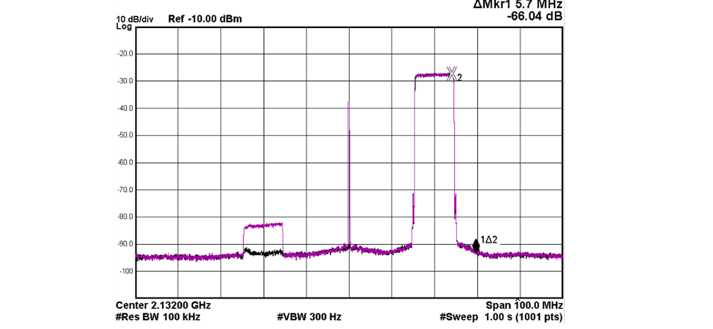
    A3. DC offset and sideband is corrected by manual which is not adaptive engine. It is not like AFE75xx (Integrated SoC). The result of manual correction is attached. Magenta is before correction and black spectrum is after correction. DC is corrected down to the noise level shown as below.

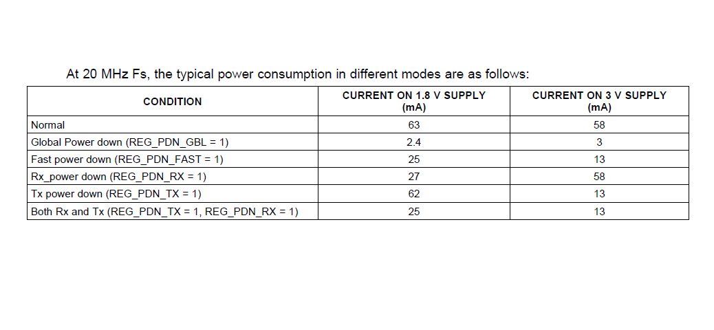
    A4. The typical power consumption is described in datasheet shown as below.

    For the maximum power consumption, it will come with full operation mode which is 245.76MHz of DAC clock and 122.88MHz of ADC clock. The measured consumption for 3.3V and 1.8V of supply was 58mA and 310mA respectively, which are 191.4mW for 3.3V and 558mW for 1.8V. The total is 749.4mW.

    A5. AFE722x has two stages of interpolation filter which has optional x2 or x4. First stage of TxFIR1 is used for x2 interpolation mode. TxFIR1 and TxFIR2 are used for x4 interpolation mode. TxFIR1 can be used HPF or LPF. Both of TxFIR1 and TxFIR2 can be set as LPF or HPF. TxFIR1 has 43-tap and stop band attenuation is 70dB. Pass band ripple is less than 0.1dB. TxFIR2 has 19-tap filter and step band attenuation and ripple is the same as TxFIR1. RX path also has FIR after decimation. This decimation filter consists of 43-tap and the stop band attenuation is greater than 80dB. The pass-band ripple is less than 0.1dB.

    A6. DAC dynamic range depends on Fin. For 70MHz case, datasheet says AFE7222 has 81dBc and 79dBc for AFE7225.

    A7. AFE722x is an IF-transceiver, and NF is dominantly impacted by 1st stage of RF domain. Therefore it is not specified from datasheet.


    Thanks,

    KW