This thread has been locked.

If you have a related question, please click the "Ask a related question" button in the top right corner. The newly created question will be automatically linked to this question.

ADS8556 Accuracy

Other Parts Discussed in Thread: ADS8556

Hi, folks

Our cutomer is asking us about  the ADS8556 gets unstable. The latter 2bit is unstable and someting the 3rd bit will be unstable also

even if they measured fine DC voltage. They are usning under hardware mode, and data out via serial interface.

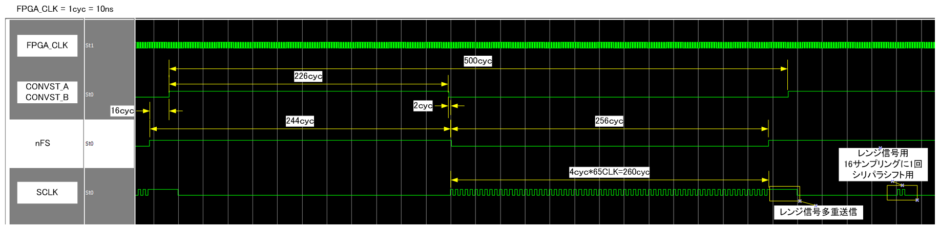
Attached figure is timing chart from customer. They uses CH_A and CH_B Only.

I got a their circuit already.  They put 0.47uF on REFIO and 10uFs on REFC_x respectively including REFC_C even if they do not used.

We are now asking to check their artwork. Especially GND around REFs.

Could you let me know if you have idea for further investigation? I guess maximin 3 bit unstable is unreasonable. Am I correct?

  • I am sorry I forget to attach.

  • Hello Keiichi Kajino-san,

    There are some aspects of the timing diagram you sent that do not make sense to me. Maybe you can help me verify whether my understanding is correct:

    1)      It seems that the CONVST_A and CONVST_B pins are held high for 226 FPGA clock cycles. Could you explain why are they keeping the CONVST_A and CONVST_B signals high for such a long time? The reason I ask is because I would expect the CONVST_A and CONVST_B pins to be brought low after the FPGA detects the BUSY pin going low. Since the maximum conversion clock period is 68 ns, I would expect the CONVST_A and CONVST_B signals to be high no more than 1.3 us. Could you explain to me what is the customer’s algorithm to control CONVST_A and CONVST_B?

    2)      Unless I have incorrectly interpreted the timing diagram, it looks like your customer synthesizes the SCLK by using 4 FPGA clock cycles. Could you please confirm that this is the case?

    3)      Another aspect that is not clear in your forum post is: could you tell me whether your customer is using SDO_A and SDO_B or only SDO_A? What are the states of pins 15, 16 and 17?

    4)      Since your customer is using CH_A and CH_B only, could you clarify why are they transmitting 65 SCLK cycles during the frame synchronization period?

    5)      What is the level connected to pins 1, 27 and 63?

    6)      I do not fully understand what you mean by “The latter 2bit is unstable and someting the 3rd bit will be unstable”. Could you please send me more information on that subject? I would appreciate if you told me what the analog input is in your test and what is the serial bit-stream coming out of the converter. Please highlight which bits in the bitstream you are calling 2nd bit and 3rd bit.

    Best regards,

    Jose

  • Hello Jose, Thank you for your reply.

    I update as follows. I will update 1) and 6) after I get info from customer.

    1) I am checking with customer.
    2) Yes, they are using 10ns of FPGA clock and provide 4 cycle clock as SCLK. (Uses internal clock for conversion)
    3) They uses both CH_A and CH_B. The 15, 16 and 17 pins are tied to GND.
    4) At previos another thread, We got answer that the SCLK should be high when @(posedge nFS). So 1st SCLK is for this.
    5) The 1 pin is tied to GND. The 27 and 63 pins are tied to BVDD.
    6) I am checking with customer.
  • Hello, Jose

    I got answer from customer.

    1) They are not supervising BUSY signal. They add 1us from 1.26us. So CONVST_x high period will be 2.26us currently.
    We guess enough convertion time does not affect measurement result.

    6) Input 78'dec signal, measurement result will be 45 to 111.
    78'dec = 8'b0010110, 45'dec=00101101, 111'dec=01101111. So over 3bit LSB gets unstable.
  • Hello Keiichi Kajino-san,

    Thank you very much for the additional information. However, there are still some answers that are very puzzling.

    The one that concerns me the most is when you wrote: “They uses both CH_A and CH_B. The 15, 16 and 17 pins are tied to GND.”

    As indicated in the ADS8556 datasheet (please read pages 4 and 5): “DB0/SEL_A Pin 17, serial mode, Select SDO_A input. When high, SDO_A is active. When low, SDO_A is disabled. Must always be high.” Please ask your customer to change their schematic and board layout to ensure that pin 17 is tied to BVDD; otherwise, they will not be able to read data in serial mode properly. Also, could you please verify whether they are connecting pin 61 to BVDD?

    The other point that I do not understand is when you say: “Input 78'dec signal”.

    Perhaps you can ask the customer for the analog voltages (as in how many volts dc) they are applying on pins 33, 36, 39 and 42 when they run the experiments. Also, could your customer attach oscilloscope plots of the voltages on these three pins? Also, could you please include a schematic of the circuitry connected to pins 33, 36, 39 and 42? Thank you.

    The other points in your reply seem OK to me.

    Best regards,

    Jose

  • Jose,

    I am sorry I made a mistake, but the pin17 is surely connected to BVDD.

    I am asking true voltage on CH_Ax and CH_Bx via oscilloscope. I will update when I get data.

    As for schematic, since this is customer sensitive info, I can not put it on open discussion.
    Could you send your e-mail address to me (keiichi_kajino@ktl-corp.co.jp)? and then I will send it you directory.

    Thanks always.