This thread has been locked.

If you have a related question, please click the "Ask a related question" button in the top right corner. The newly created question will be automatically linked to this question.

what is the exact formula to find the RTD_Value from ADS1247 adc. i am using 3 wire RTD

Other Parts Discussed in Thread: ADS1247, ADS1248, ADS1248EVM-PDK

hi,

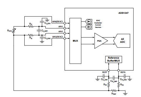
i am using ADS1247 for sensing the Temperature. i am using 3 wire RTD sensor. to find the RTD resistance what is the exact formula?

  • Hi Pattan

    that depends on your circuit implementation and ADC configuration. The following reference design shows one possible solution for a 3-wire RTD measurement system and describes how to calculate the RTD resistance.

    Please let us know in case this is not helpful and you would need further guidelines.

    Regards,

  • i am using the same design as you mentioned in your reply. i am also sending the pic of design in the attachment. my question is how to calculate the Temperature from the output of ADC (24 bit data) and also how to calculate RTD resistance from the output of ADC. i want the formula to calculate both.

  • Pattan,


    First you use the ADC to calculate the resistance of the RTD, then you use the resistance to get the temperature (either through a lookup table or by calculating it from an equation).

    To get the resistance value of the RTD, you must first use a precision resistor for the reference resistor RREF. Current flows from the excitation current sources to each lead of the RTD and then through the reference resistor. The output code of the ADC becomes:

    Output code = (RRTD*2^23)/(2*RREF)

    This assumes that the ADC PGA gain is 1. If the reference resistor is known and accurate, then you can calculate the equivalent resistance for the RTD. As an example, here is a lookup table for a PT100 RTD:

    www.omega.com/.../z252-254.pdf

    Alternately you can use the Callendar-Van Dusen equation to calculate the temperature from the resistance:

    www.omega.com/.../RTDSpecs_Ref.pdf

    Note that the TI design that Joachim mentioned does require calibration. Achieving precision results will requires attention to a lot of the details that make up the circuit. If you do try to duplicate this design read through the writeup carefully to make sure you understand what is required to get the desired accuracy.


    Joseph Wu
  • Hi Joseph Wu,

    i have  configured the ADC by writing data into the Registers like MUX0,  MUX1,  SYS0, IDAC0, IDAC1, GPIOCFG, GPIODIR and GPIODAT but

    1). how to Read The 24 bit Output from the ADC? which Command i have to give to get the Output?

    2).whether if i gave a command, can i get the 24 bit data automatically? or i can read 3 bytes of data separately?

    3). In Your Previous Reply you have told me the formula to calculate RRTD,

                
    Output code = (RRTD*2^23*PGA)/(2*RREF)

    here PGA=4, RREF=820 ohms and let RRTD= 157.33 ohms for that RRTD i have to get a Temperature of 150 degree centigrade. if a submit  these values in the formula then i get a code 0x311E1E . then how Could i get 150 Degrees with this formula?

    4). what is the purpose of OFC Registers. i did not understand that registers functionality

  • Pattan,


    I'll answer questions 1 and 2 together. When the ADS1248 is powered up, the default mode is read data continuously. This means that each time the ADC completes a conversion, the data is put onto DOUT to be read out. In this mode, you can monitor /DRDY and use it as an interrupt to clock out data, without issuing a command. You can simply give the device 24 SCLKs to read the data. Note that you need to monitor /DRDY. If you are in the middle of clocking out data, and the ADC completes a new conversion, the ADC will update DOUT in the middle of your read. This will result in wrong data where the result is a combination of the first bits of one conversion, and the first bits of the newly completed conversion.

    An alternate way to get the data is to put the data in stop read continuous mode. First you issue an SDATAC command. The ADC will continue to do conversions, but it no longer automatically updates the DOUT with a new conversion. To get the data, you issue an RDATA command and clock in 3 NOPs (24 SCLKs) to read the data. If you cannot easily monitor /DRDY, I recommend using the SDATAC mode.

    You use the equation to get the resistance of the RTD from the output code of the ADC. Then you use the resistance of the RTD to get the temperature.

    If you have the RTD resistance, you can use either a lookup table or solve the polynomial from the Callendar-Van Dusen equation. The links I provided in the last post should be able to guide you to getting the temperature. If the temperature is over 0°C, you can solve for temperature using the Callendar-Van Dusen equation with the quadratic equation. The ADC does not provide direct temperature conversion.

    The OFC is the offset calibration register. Even though the input amplifier/ADC has an built-in offset correction, there is still a residual offset remaining in the measurement. If you run a SELFOCAL (self offset calibration), the device will internally short the inputs and store a code in the OFC. This value will be subtracted from future conversions to eliminate this offset. Generally you would set the device in the configuration that you would be operating it in, send the SELFOCAL command once and then run the device.


    Joseph Wu
  • Hi,

    Can u please explain me briefly the second approach of reading ADC? I want the syntax of command. I.e the sample code. How to issue that command and how to provide NOPs?

  • Pattan,

    If you are able to read and write to the registers, you should be easily able to read data back from the device.

    There is some code that is used for the ADS1248EVM-PDK, and you can find that in one of the older posts here:

    I'm not sure if the code uses a RDATA command, but surely it uses a RREG command which will be similar.

    The code may be a bit complicated to follow so I'll include my own example.

    To communicate with the ADS1248, the /CS is low to enable the SPI, SCLK dwells low and data is clocked in (or read) at the falling edge of the SCLK, MSB first. The example drawing I have here is using RDATA (12h) clocked into the device and then a series NOPs to clock out the data on DOUT. Here the example figure clocks out 311E1Eh as in the code example you mention in a previous post.

    Dotted lines separate the bytes, but in operation, bytes do not need to be separated to extra time.

    Joseph Wu

  • Hi Joseph Wu,

    As you Mention i write the following code. Please Check the format of the code is correct or not.

    After Getting DRDY pin output as LOW

    first i issue a command SPI_Tx(0x16); // SDATAC Command (Stop reading data continuously)
    then SPI_Tx(0x13); // RDATA Command 0x13 (Read data once Command)
    then

    SPI_Tx(0xFF); // NO OPERATION NOPs 0xFF three Times
    SPI_Tx(0xFF);
    SPI_Tx(0xFF);

    then

    i have taken unsigned char RxByte1 = 0x00, RxByte2 = 0x00, RxByte3 = 0x00;
    unsigned int Output2 = 0x00000000;

    RxByte1 = SPI_Rx();
    RxByte2 = SPI_Rx();
    RxByte3 = SPI_Rx();


    then i join the three Bytes as below

    Output2 = RxByte1<<16;
    Output2 = Output2|(RxByte2<<8);
    Output2 = Output2| RxByte3;


    is this the Correct Approach?
  • Pattan,


    In general, this looks correct. I just want to point out a few things to remember.

    First, /CS should be low for the duration of the transaction. Second, The NOP transmission and the read data are the same 24 SCLKs. NOPs are used to clock out the data. Finally, data is clocked out MSB first.

    When implementing this system, I highly recommend using an oscilloscope or logic analyzer to look at the signals. It helps to see the actual digital transaction when trying to debug the code and nothing works.

    The diagram of the communication that I put in the last post is useful when you are able to see the digital communication.


    Joseph Wu
  • Hi Joseph Wu,

    i am trying to write data into ADC GPIODAT Register, but the SPI Communication is not writing data. here i am providing  my code. Please Correct me.

    ADC_Write(0x4C,0x00,0x0F); // Selecting as GPIO
    Delay(0x0F);
    ADC_Write(0x4D,0x00,0x00); //Selecting as Outputs
    Delay(0x0F);
    ADC_Write(0x4E,0x00,0x0F); //writing four bits as 1's
    Delay(0x0F);

    while reading the Register i am not getting data what i wrote

    Temp=ADC_Register_Read(0x2E,0x00);

  • Pattan,


    I don't see anything specifically wrong with how you have the write and the read set up. It appears to go to the proper register, write one byte, and gives the single byte to be read.

    However, problems like this are best viewed with an oscilloscope or logic analyzer. This way you can see the exact transaction you are sending. Getting something to look at the communication lines is essential to debugging the ADC transactions.


    Joseph Wu