Hi,
I am working on a project in which we have designed a board which contains CC2541 and multiple sensors interfaced to it via spi like temperature,accelerometer , ADS1293 and also a sd card for data logging.Currently device is supplied with the cc debugger only.
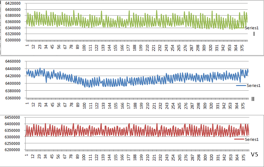
I have implemented 5 lead application for ADS129 and collected the data from the ads1293 by connecting 5 electrodes(RA,LA,LL,RL,V5) to the body and entered this data in the excel sheet and plotted a graph and i got the graph as given in the below image.
Register settings:
(0x00,0x00); // Stop data conversion.
(FLEX_CH1_CN,0x11); // Connects channel 1’s INP to IN2 and INN to IN1.
(FLEX_CH2_CN,0x19); //Connect channel 2’s INP to IN3 and INN to IN1.
(FLEX_CH3_CN,0x2E); // Connects channel 3’s INP to IN5 and INN to IN6.
(0x04,0x00);
(0x05,0x00);
(0x06,0x00);
(0x0a,0x07); //Enables the common-mode detector on input pins IN1, IN2 and IN3.
(0x0c,0x04); //Connects the output of the RLD amplifier internally to pin IN4
(0x0d,0x01);
(0x0e,0x02);
(0x0F,0x03); //Connects the first buffer of the Wilson reference to
//the IN1 pin, the second buffer to the IN2 pin, and the third buffer to the IN3 pin.
(0X10,0x01); //Connects the output of the Wilson reference internally to IN6.
(0X11,0x00); //Internal VREF turned ON
(0x12,0x04);
(0x13,0x00); //DEFAULT
(0x14,0x00);
(0x15,0x00);
(0x16,0x00);
(0x21,0x02); //Configures the R2 decimation rate as 5 for all channels.
(0x22,0x10); // Configures the R3 decimation rate as 16for channel 1.
(0x23,0x10); //Configures the R3 decimation rate as 16for channel 2.
(0x24,0x10); //Configures the R3 decimation rate as 16for channel 3.
(0x25,0x00);
(0x26,0x00);
(0x28,0x00);
(0x29,0x00);
(0x2a,0x00);
(0x27,0x08); // Configures the DRDYB source to ECG channel 1 (or fastest channel).
(0x2F,0x71); // Enables ECG channel 1, ECG channel 2, ECG channel 3 and Data Status for loop read-back
mode.
Data Rate : 320 samples/sec
Cvref : Internal Reference voltage i.e. 2.4Volts.
The waveforms are not proper.I think there is lots of noise.What should i do to remove the noise?I have followed ti reference design while designing the circuit for ADS1293.
Also note that at every 1.5 sec i am stopping the data conversion as need to write the data into the sd card as soon data writing is completed i am restarting the conversion,if i don't stop the conversion before writing into the sd card, the device fails to write data into the sd card.
please give your suggestion on this.