This thread has been locked.

If you have a related question, please click the "Ask a related question" button in the top right corner. The newly created question will be automatically linked to this question.

ADS7844E is not working properly

Other Parts Discussed in Thread: ADS7844

HI all

We are using ADS7844E in our application through SPI interface but it is not working properly?

  • Hello Shivakumar,

    The information provided in the query is not sufficient to provide any suggetsions to resolve your issues.

    Please share mode information regarding the issue observed.

    e.g. The converted data does not match input
    or the channel selection not working etc.

    Please share the commands you are passing to the device as well.

    Thanks & Regards,
    Shridhar.
  • Hi shridhar

    Thank you for the reply. we interfaced ADS7844E with PIC Microcontroller through SPI. We are able to see the data reaching upto the ADC pin. we are writing 0x97 for the second channel but data we are getting is constant despite we varied through potentiometer.

    Please find the attachment and our code below.

    void InitSPI()
    {

    SPI2CON1bits.DISSCK = 0; //Internal Serial Clock is Enabled.
    SPI2CON1bits.DISSDO = 0; //SDOx pin is controlled by the module.
    SPI2CON1bits.MODE16 = 1; //Communication is byte-wide (8 bits).
    SPI2CON1bits.SMP=0; //Input Data is sampled at middle of data output time.
    //Serial output data changes on transition from idle clock state to active clock state
    SPI2CON1bits.CKE = 0;
    //Idle state for clock is a low level; active state is a high level
    SPI2CON1bits.CKP = 1;
    SPI2CON1bits.SSEN=0; //SSx Pin not used by the module
    SPI2CON1bits.MSTEN = 1; //Master Mode enabled
    SPI2CON1bits.SPRE=0b001; //Secondary prescalar is 4:1 //FCY is 20MHz
    SPI2CON1bits.PPRE=0b11; //Primary prescalar is 1:1

    SPI2CON2bits.FRMEN=0; //Framed SPI support is disabled

    SPI2STATbits.SPIEN=1; //Enable SPI Module
    SPI2STATbits.SPISIDL=0; //Continue Module operation in idle mode
    SPI2STATbits.SPIROV=0; //Receive overflow flag is cleared


    }

    unsigned int SPI_Recieve(void)
    {
    SPI2STATbits.SPIRBF=0;
    SPI2BUF=0x00;
    while(!SPI2STATbits.SPIRBF);


    return SPI2BUF;
    }

    void SPI_Send(unsigned char Data)
    {
    SPI2BUF=Data;
    while(SPI2STATbits.SPITBF);
    while(!SPI2STATbits.SPIRBF);
    Data=SPI2BUF;

    }

    main(){
    char ControlByte, Start;
    int Data;

    while(1){


    //ch 0 = current. ch 1 = feedback. ch 2 = voltage

    Start = 0x87;
    ExternalADC_CS = 0;
    ControlByte = Start | (channel << 4);
    SPI_Send(ControlByte);
    // Delayus(500);
    Data = SPI_Recieve();

    ExternalADC_CS = 1;

    }

    }

  • Hello Shivakumar,

    The register content you are sending as control word is correct for the SGL mode CH2 data capture.

    It appears you are using DCLK frequency as 20MHz. The device can operate at maximum DCLK = 2.5MHz for 3.3Vcc & 3.33MHz for 5V Vcc.

    Due to high DCLK frequency the timing specifications for ADC are getting violated. Please change the DCLK frequency to satisy the timing requirements mentioned in Table VI or VII according to your Vcc.

    Thanks & Regards,
    Shridhar.
  •  hello shridhar

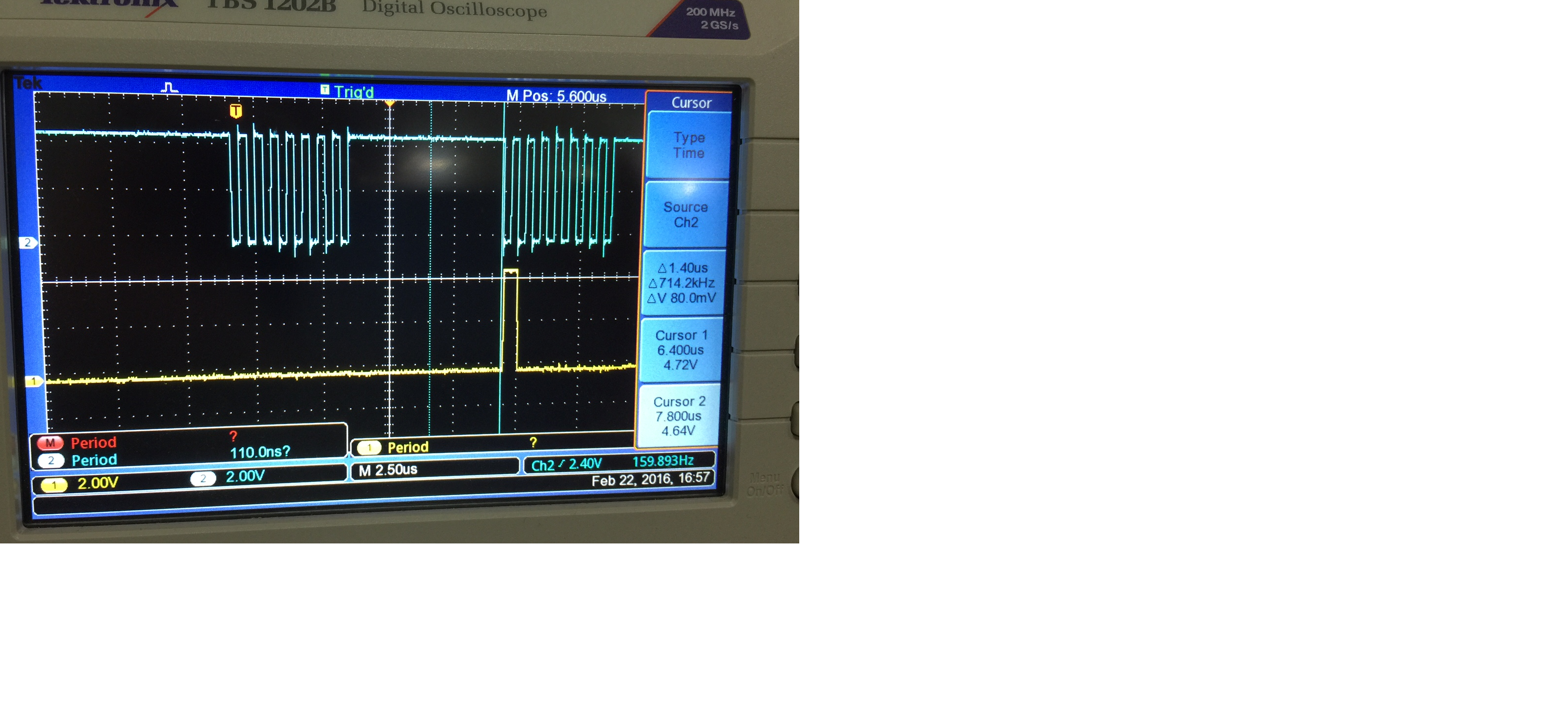
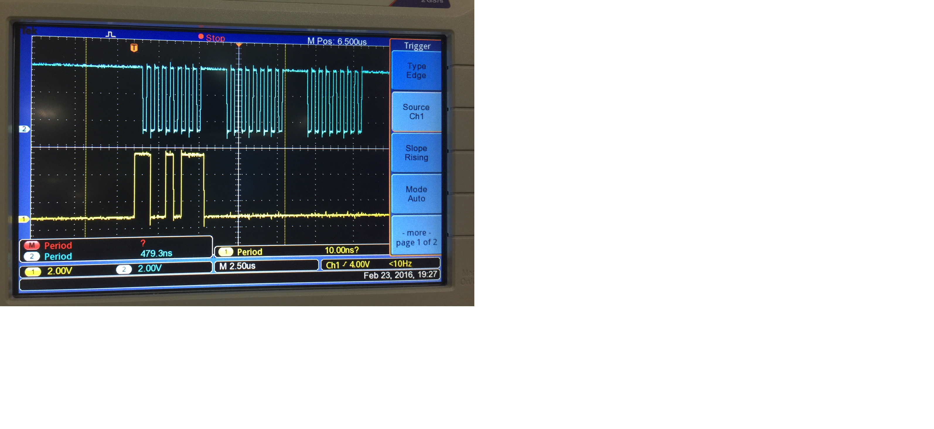
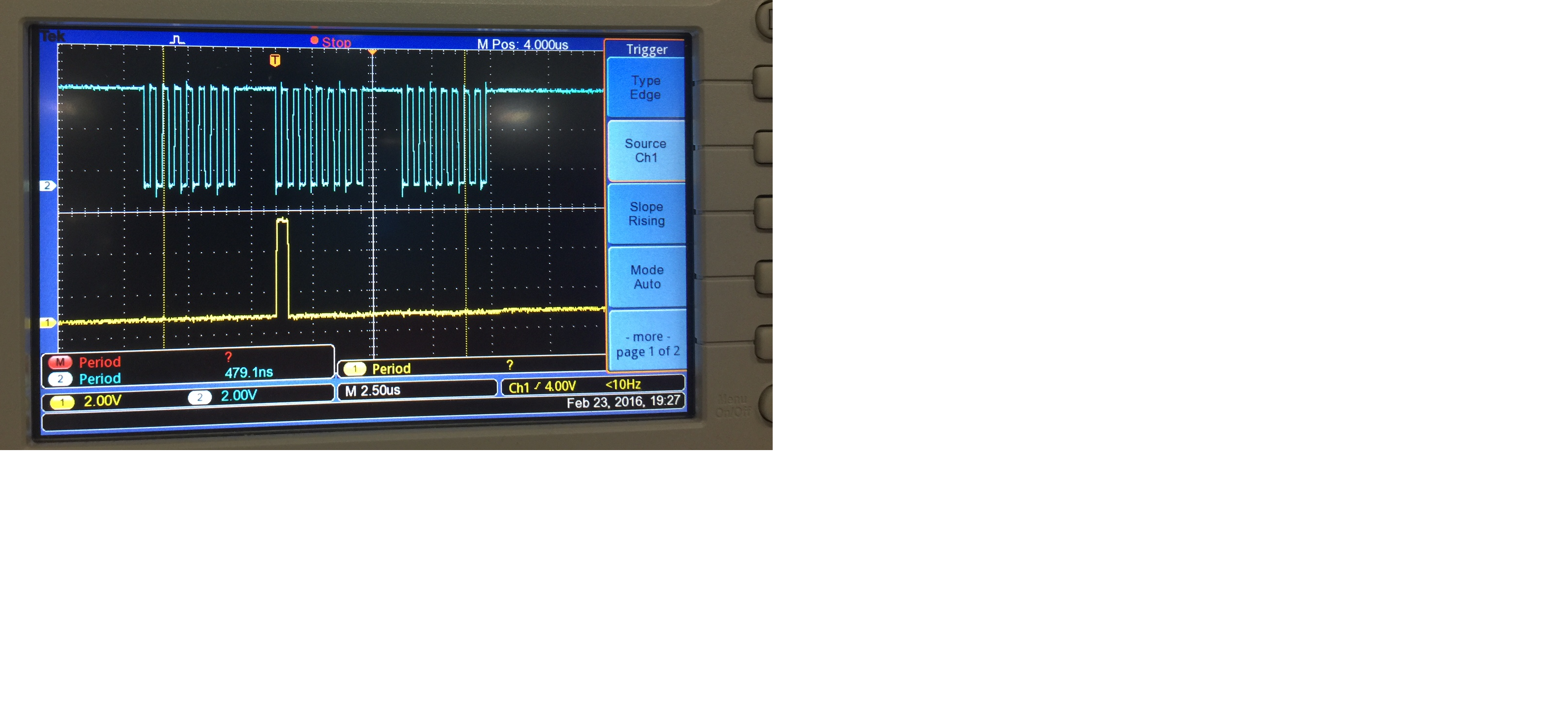
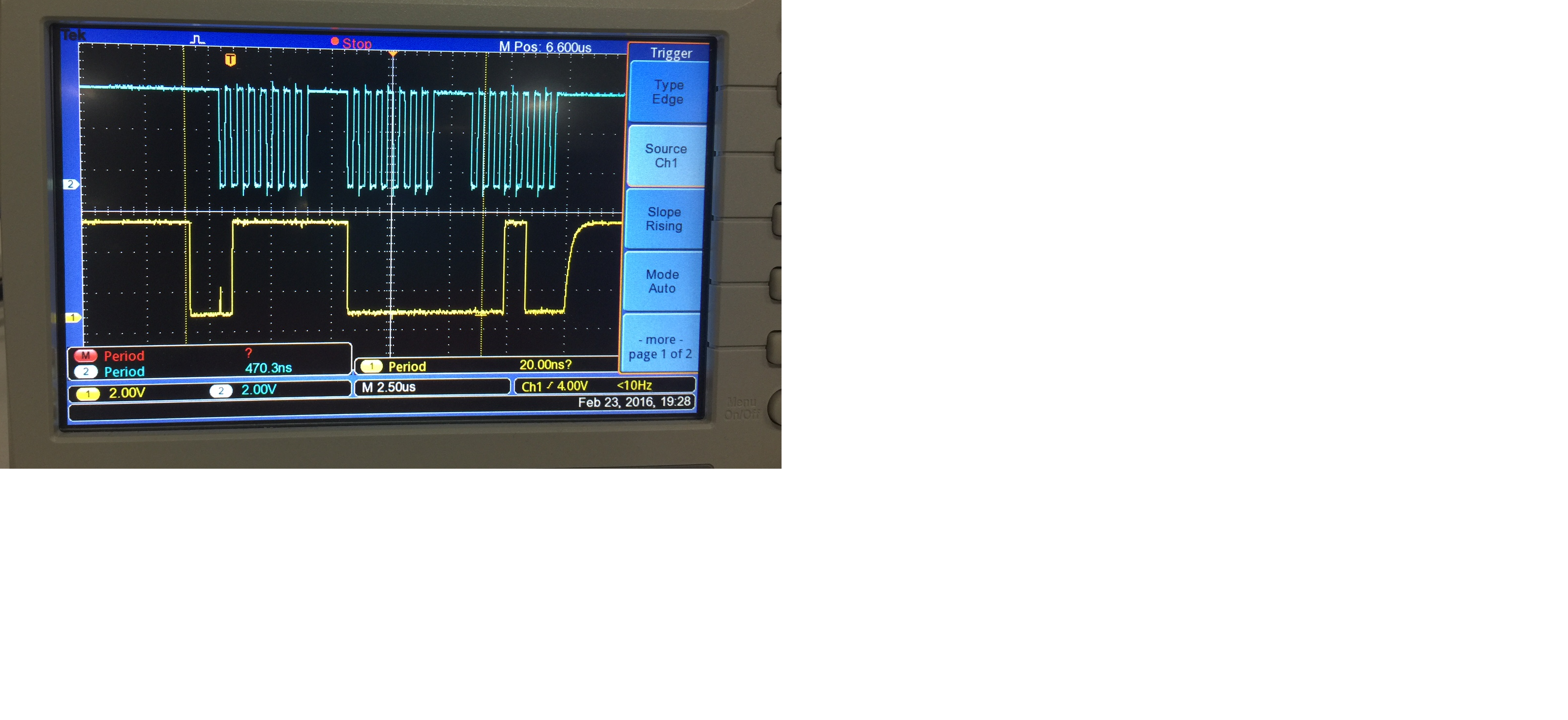
    Despite  change in frequency of DCLK from 5MHz to 1.7MHz still we are getting same frustrated results.please find the waveform below of both Data in and Data out.

  • Hello Shivakumar,

    Below are my observations from the waveforms shared & my comments regarding the same. Please correct if my observations are correct.

    1. I am assuming CS is held LOW for 3 bytes i.e. 24DCLK (1 byte for DIN programming & 2 bytes for data capture). I do not see the CS here & hence I assume that it is LOW when the SPI transaction is ongoing.
    2. The 1st image shows DCLK starting & ending in LOW state, while the 2nd image shows DCLK starting & ending in HIGH state. I do not know why these are different. Please confirm if CS is being pulled HIGH between device programming & data capture. If yes, can we avoid that.
    3. Please check if BUSY goes high after DIN 8th bit has been transmitted & goes LOW from the next DCLK.
    4. The device latches the information from DIN pin on the rising edge of DCLK. The DIN value should toggle at the falling edge of DCLK. The 1st image shows that the DIN data is toggling when DCLK is rising. This needs to match the device timing diagrams.
    5. Please confirm if the issue is observed across multiple devices of ADS7844.
    6. Please confirm the reference & power supply inputs are stable during the ADC conversion.

    Please make sure the digital interface is matching all the timing requirements or timing diagrams are met according to the datasheet.

    Thanks & Regards,
    Shridhar.
  • Hi shridhar

    Please find attachment our captured waveform 

    1. chip-select with clock

    2. clock with data in with respect to ADC

    3. clock with busy with respect to ADC

    4 clock with Dout with respect to ADC

     https://e2e.ti.com/cfs-file/__key/communityserver-discussions-components-files/73/waveform.7z

  • Hi shridhar

    we noticed that data out from ADC is not changing(always constant) with respect to change in  input.

  • Hello Shivakumar,

    Based on the images shared the SPI mode used by the controller is CPOL = 1 & CPHA =1.
    The device ADS7844 works with CPOL = 0 & CPHA = 0 configuration i.e. DCLK should be LOW when CS pin goes LOW & the device latches the data on DCLK rising edge. Please refer figure 3 & 4 of the datasheet.

    Please change the mode setting for the controller SPI.

    Thanks & Regards,
    Shridhar.
  • Hi shridhar

    we tried all four possibility with CPOL & CPHA (00,01,10,11) but we are not getting expected output.

  • Hello Shivakumar,

    I will need more information now to get to the cause of the issue. I will initiate a private discussion with you regarding the same. You can share additional discussion in those communications.

    Meanwhile, please confirm if the issue is observed with multiple ADS7844 devices while working with SPI mode 00.
    Also, check if the refernece & power supply are at expected voltage levels.

    Thanks & Regards,
    Shridhar.
  • Hi shridhar

    Please let me know what kind of information do you required? This is our prototype design it has to go for production in may. we have to freeze the design as early as possible.

    for your above query

    we are getting 4.97V at VCC and 4.99V at Vref

  • Hello Shivakumar,

    After updating the SPI communication, the issue is resolved. Please reconfirm and I will close the communication.

    Thanks & Regards,
    Shridhar.
  • Hi shridhar

    after updating SPI it is now working fine.