This thread has been locked.

If you have a related question, please click the "Ask a related question" button in the top right corner. The newly created question will be automatically linked to this question.

ADS8684 commands

Other Parts Discussed in Thread: MSP430F249, ADS8684, ADS8668, MSP430F2274

Good afternoon,


I'm working with ADS 8684 and the MSP430F249.
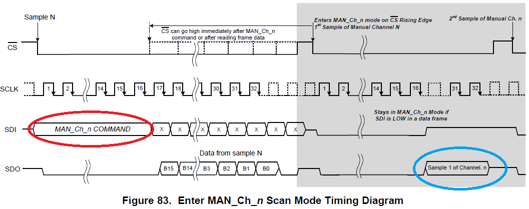
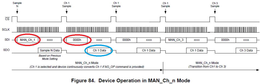
It is possible to tell me the sequence of commands to the ADS8684 be in manual mode.
For example:
I intend to read the channel 0 manually.
What is the sequence of commands to send to the ADS8684?


Best regards

  • Hi Carlos,

    To get the data  on the channel you want, two complete frames of 32 SCLK cycles should be implemented on SPI bus:

    1. Write a valid manual channel n select command(MAN_Ch_n in red circle) into the command register with 32 SCLKs.

    2. Send No_OP command(0000h) with another 32 SCLKs because the conversion will be activated on the falling eage of /CS, the analog input signal on the channel selected in the previous framel will be converted during this particular frame. The converted data will be retrieved in this particular frame(blue circle).

    Please refer to the timing diagrams as below:

    Please let us know if you have more questions. Thanks.

    Best regards

    Dale Li

  • Hello Dale Li,


    Thanks for your response.

    I'm doing exactly what I stated and 5V analog input the amount you get after conversion is always in the range of 30000.

    The dispositvo is configured with the default settings.

    Do you have any solution to my problem?

    Best regards

  • Hi Carlos,

    Can you please upload your schematic here? It will be very helpful as well if you can upload the screenshot for SPI timing you meansured on /CS,SCLK,SDI and SDO. By the way, ADS868x device uses SPI serial communication in mode 1 (CPOL = 0, CPHA = 1). Thanks.

    Best regards

    Dale Li

  • Hello Dale Li,

    I thank your time.

    Soon she sent him the CS curves, SCLK, SDI and SDO.
    First of all, I would like to observe my wiring diagram to see if there is a problem.

    Note: I plan to use only one ADS8684 with its internal reference.

    Best regards


  • Hi Carlos,

    One problem for this schematic, the decoupling capacitor on REFIO should be at least 10uF, but 1uF(C148) is used in this circuit. Please modify and check again.

    You have two grounds, GND and GNDA, I would like to see the pcb layout, and wait for the timing screenshot as well. Thanks.

    Regards

    Dale

  • Hello Dale Li,


    CS curves, SCK, SDI and SDO only'll get next week.
    I use GND (Digital) and GNDA (Analog), as shown in the following diagram:


    Greetings.

  • Hello, I'm using ads8668, i have a problem in enabling the ADC, Even after giving all the power supply(AVDD and DVDD) , i don't get logic high value at the pin CS bar. Compared to the above circuit, my circuit was little different, REFIO and REFCAP are connected together and grounded with 22nf + 10nf in parallel. And as i'm using only one input channel, i din't ground the other analog input ground pins. But the pins 33,32,31,29,28,8 are grounded. So my question is should i ground all gnd pins to ground? And do you find any problem in my connection?
  • Hi Jay,

    Please open a new post with your questions and detailed information including schematic. Thanks. One problem I find from your simple description is, REFIO and REFCAP pins shoud be decoupled separately, please refer to the recommendations in Figure 73 with internal reference and Figure 78 with external reference. By the way, Pin CS is input pin, I don't know why you want to get logic high value on this pin.

    Thanks.

    Regards

    Dale Li

  • Hi Carlos,
    Looks like your have three grounds, GNDA,GND and GND_IN. Where is the Ground connection? especially GNDA and GND, I can't get the information from this simple diagram.
    Please correct the cap on REFIO with least 10uF and let me know the result.Thanks.

    Regards
    Dale Li

  • Hello Dale Li,

    Thanks for your response.

    Already replaced the 1uF capacitor for a 10uF.

    My SPI configuration:
    SPI_MODE1 (CPOL = 0, CPHA = 1)
    clock source = UCSSEL_2
    clock divider = 5

    My ADS8684 configuration:
    Keep the default setting.
    Vref = 4,096
    input voltage range is ± 10V (± 2.5VxVref)
    Channel 0 in manual mode

    The results obtained are:

    AIN_0P ADC [range]
    0V 30000
    5V 15000

    The electrical schematic is as follows:


    Thank you
    Greetings

  • Hi Carlos,

    The problem to cause wrong conversion code is, your REFGND(Pin 6) is floating and it should be connected to analog ground, please refer to datasheet. Check the voltage on REFIO and REFCAP to make sure correct.

    I still can't get any information for your GNDA and GND because of no pcb layout and I don't know where is the Ferrite bead's position on the pcb board. The guide line is, the joint point should be close to ADC or a whole ground plane can be used and keep the ground clean.The improper design will degrade the performance.

    By the way, Pin 4 should be connected GND if you split the ground. C152 on AVDD pin should be connected to ground for decoupling purpose.

    Best regards

    Dale

  • Hello,

    Regarding the ADS8684, I discovered that my problem was to use the spi mode CPOL = 0 and CPHA = 1. When I put the spi mode CPOL = 0 and CPHA = 0, I managed to read the ADS8684 data correctly.

    Thank's for your time.

    Carlos Martins

  • hi Carlos,

    i am trying to do the same as you with msp430f2274, you can help me with the code. You can send your code to analyze it and do the same with the msp430f2274. thank you very much.